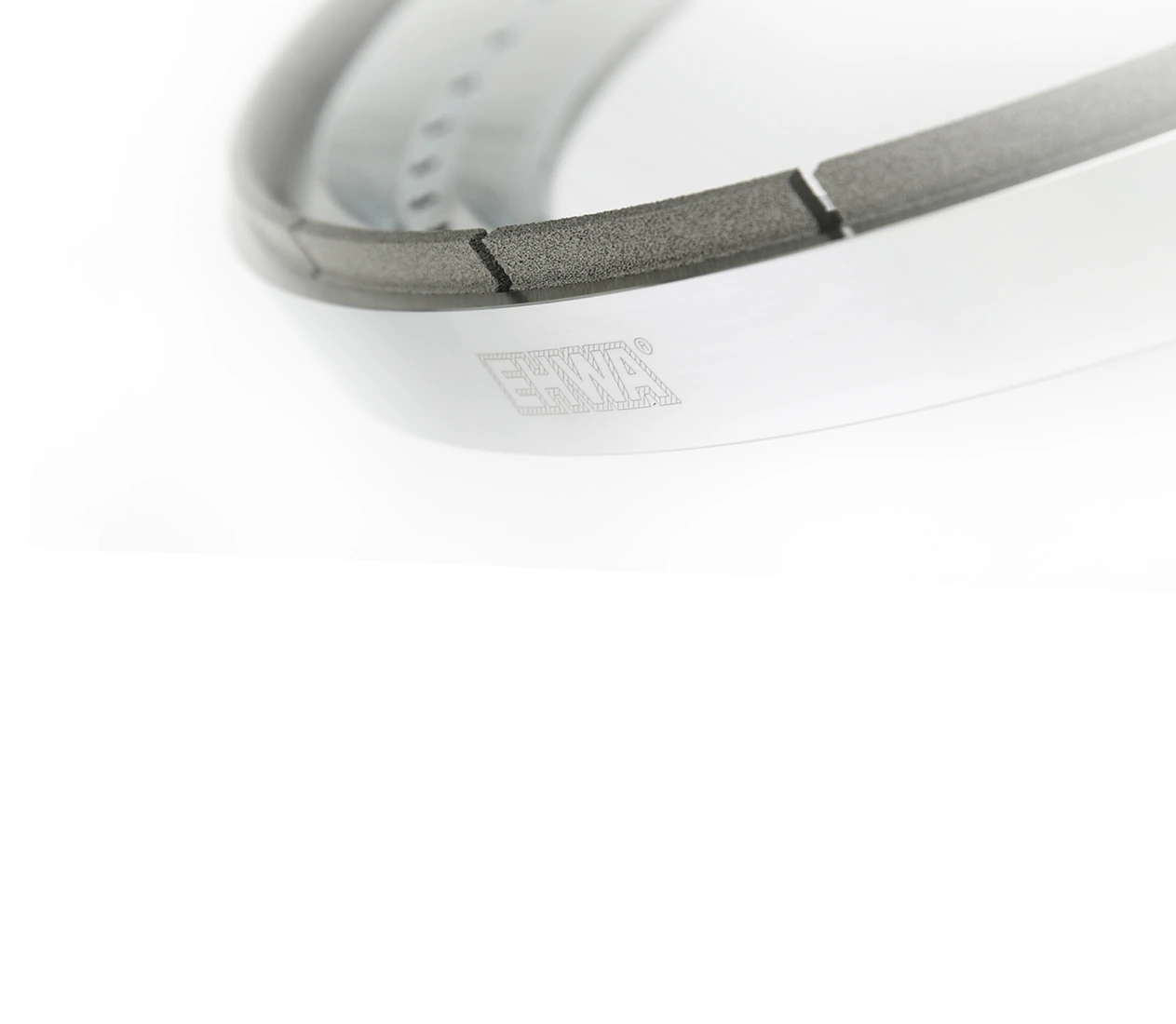
NANOPOL for wafer and compound processing
NANOPOL is an EHWA vitrified-bond tool family for back grinding. The sources explicitly distinguish silicon wafers from compound wafers. Material structure, required surface finish and processing stage determine the appropriate tool design.
EHWA describes controlled diamond distribution and adjustment of porosity, pore size and pore shape. These features can support surface quality and die strength while reducing grinding load and edge chipping. Selection links the required quality with feed rate, grinding current and useful wheel life.
Applications and process stages
| Task | Tool relationship | Important consideration |
|---|---|---|
| Rough grinding silicon wafers | NANOPOL Z1 design | Removal, current and surface after Z1 |
| Fine grinding silicon wafers | NANOPOL Z2 design | Roughness, remaining damage and useful life |
| Grinding compound or moulded wafers | Matched vitrified design | Combination of softer and harder constituents |
| Grinding moulding material with silicon and metal | Tool matched to the compound structure | Adhesion of polymer, copper or solder constituents |
Rough and fine grinding are considered together. The surface left by Z1 establishes the starting condition for Z2. A tool comparison should therefore connect the required result and existing process sequence rather than rely on a single measurement.
Match the bond structure to the material
For silicon grinding, the source describes wear and the exposure of new abrasive grains as part of the working mechanism. Compound wafers frequently contain softer or ductile constituents that can adhere to the tool surface. This changes the requirements for bond behaviour and free-cutting performance.
EHWA presents different wheel structures for these tasks. Bond bridge design and bond content are used to help remove adhering material from the working surface. Useful tool life is deliberately considered alongside grinding ability and finish. The most wear-resistant design is not necessarily the best answer to a compound process in which the wheel becomes loaded.
The documents list several specification families for Z1 and Z2. These remain EHWA tool codes and are not translated into universal grit or bond properties without a manufacturer definition. The complete specification, tool dimensions and actual application provide the basis for selection.
Catalogue example: Z2 on a DGP8761
The silicon wafer document presents two Z2 designs on a DGP8761. The following values were checked against the original page:
| Reported measurement | 5000-VKBT25 design | 8000M-VNPSSR design |
|---|---|---|
| Feed rate | 0.6 µm/s | 0.2 µm/s |
| Grinding current | 13.5 A | 15.5 A |
| Useful wheel life | 23,000 pieces | 4,500 pieces |
| Ra roughness | approximately 4.8 nm | approximately 1.3 nm |
| Rmax roughness | approximately 56 nm | approximately 15 nm |
Source: NANOPOL silicon wafer document, original PDF page 9. Roughness is reported using a Wyco Veeco NT9100. The designs have different specifications and feed rates. The table illustrates the relationship between finish, operating conditions and useful life; it is not a comparison under identical conditions or a setting instruction for other machines.
Selection begins by establishing the required finish and available processing time. A suitable design can then be discussed in relation to the existing stages and material structure. For compound wafers, the tendency of constituents to adhere to the wheel is an additional selection factor.
Discuss your grinding task with EHWA
Provide the wafer material or compound structure, diameter, initial and final thickness, machine and existing Z1/Z2 tools. Feed rate, grinding current, surface measurements and wheel life support the comparison. Start with the information already available and use the technical discussion to develop the remaining details. The goal is a tool design linked to a defined surface requirement and a workable manufacturing process.
EHWA Europe: info@ehwadia.de · +49 6173 997780
Sources and original documents
- EHWA: NANOPOL for compound and silicon wafers · PDF pages 1–10; Z2 example: page 9.
- EHWA: NANOPOL Compound Wafer Grinding Wheel · PDF page 1.
- EHWA: NANOPOL Si Wafer Grinding Wheel · PDF page 1.
- EHWA: NANOPOL Semicon document · PDF pages 1–4.