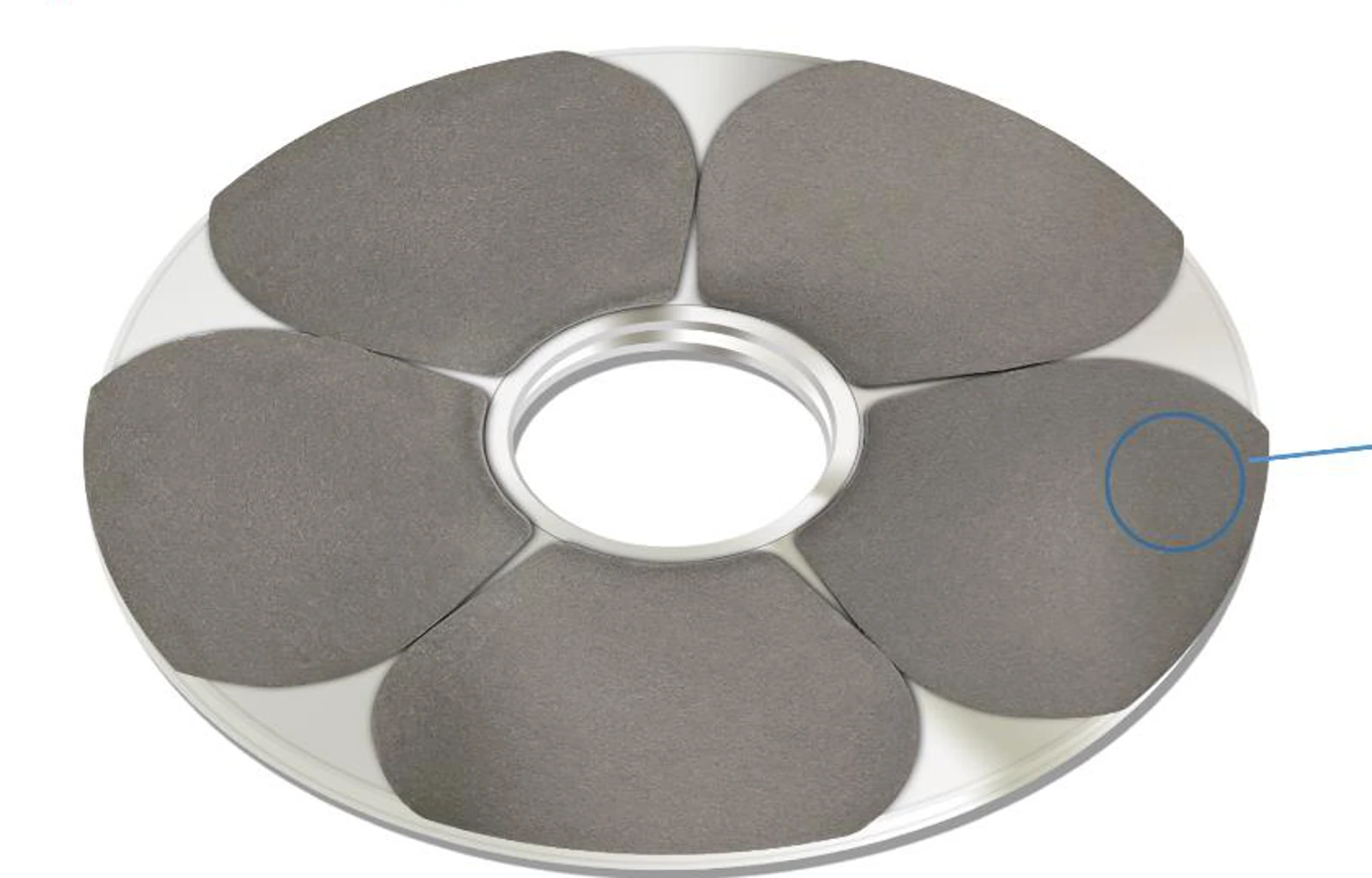
Backside finishing after grinding
EHWA presents polishing tools for finishing silicon wafers after back grinding. The sources use DP for Dry Polishing, GDP for Gettering Dry Polishing Pad and GPP for Gettering Polishing Pad. These names are considered together with the relevant tool design and source; the different names do not establish identical bonds or materials.
Backside finishing considers roughness and the damage remaining after grinding. Gettering-related processes also consider the ability of suitable structures to capture impurities. Component strength and the desired gettering behaviour are therefore considered together.
Match the tool and task
| Source designation | Task or feature |
|---|---|
| DP Wheel | Dry polishing the silicon wafer backside |
| GPP | Gettering-related polishing pad, used after Z1 and Z2 in the example |
| GDP | Gettering Dry Polishing Pad designation in supplementary sources |
| Z3 in the GPP example | Polishing tool following two back grinding stages |
Tool construction and process benefits
The DP document shows wool felt with zirconium dioxide and impregnation with resin and ZrO₂. This construction belongs to the illustrated DP design and is not transferred to every gettering pad. The tool provides a separate finishing stage after the grinding wheels.
Dry polishing operates without a polishing slurry. This process description was checked against a primary machine-manufacturer explanation. EHWA tool selection considers the equipment, mounting, preceding grinding stages and required backside quality. The actual process is defined in conjunction with the selected tool design.
GPP example from the EHWA document
EHWA presents a test with ten 12-inch silicon dummy wafers, AMC APB1-330 tape and a DISCO DGP8761. Z1 and Z2 back grinding are followed by an EHWA GPP as the Z3 tool.
| Reported measurement | Source value |
|---|---|
| Ra, centre | 0.92 nm |
| Ra, middle area | 1.05 nm |
| Ra, edge | 1.17 nm |
| Die-strength chart after Z2 | 560 MPa |
| Die-strength chart after GPP | 730 MPa |
Source: GPP document, PDF pages 1–2, visually checked. The values belong to the illustrated test. The chart does not provide a complete strength-test method, so the figures do not become a general strength or roughness guarantee.
The three roughness positions illustrate why backside finishing is assessed across different areas. A comparison also considers the surface after Z2, the tool sequence and the required gettering behaviour. This connects the final finish to the process that produces it rather than to one isolated roughness figure.
Discuss your wafer finish
Provide the wafer material, diameter, final thickness, machine, tape and existing Z1/Z2/Z3 tools. Add the required roughness, strength target and any gettering requirement. The current process sequence provides a useful starting point for selecting the appropriate finishing tool.
EHWA Europe: info@ehwadia.de · +49 6173 997780
Sources and original documents
- EHWA: GPP and DP · PDF pages 1–4; GPP test: pages 1–2.
- EHWA: GDP – Gettering Dry Polishing Pad · PDF page 1.
- EHWA: DP Wheel – Dry Polishing · PDF pages 1–4.
- EHWA: GDP, alternative test document · PDF page 1.
- DISCO: Dry polishing with polishing pads and gettering DP process · general process explanation; no third-party performance figures adopted.