CMP: chemical and mechanical action
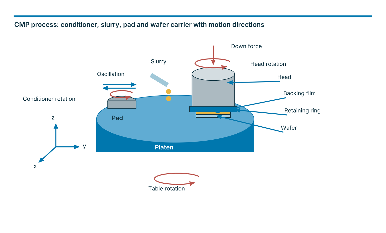
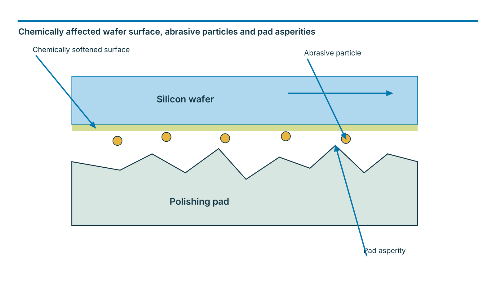
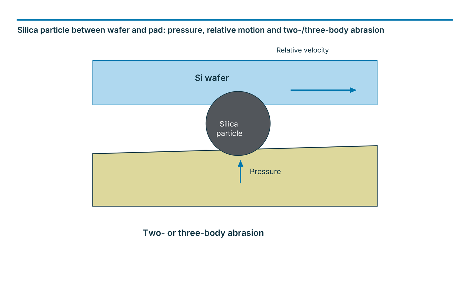
In chemical mechanical polishing, slurry, polishing pad and relative motion act together on the wafer surface. The slurry chemically modifies the near-surface layer; abrasive particles and pad asperities support mechanical removal. The process schematic uses a silicon wafer and silica particles as an example. The two- or three-body abrasion illustration describes particle contact between wafer and pad.
The wafer is held beneath a backing film in the polishing head and surrounded by a retaining ring. Down force and head rotation act on the wafer while the platen and pad rotate. Slurry is delivered to the pad surface. The conditioner rotates and oscillates across the pad; the x, y and z coordinates identify spatial directions. Conditioner motion and wafer-carrier motion perform different functions within the same process.
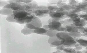
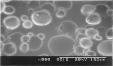
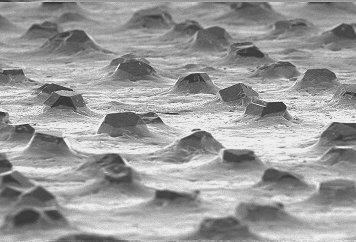
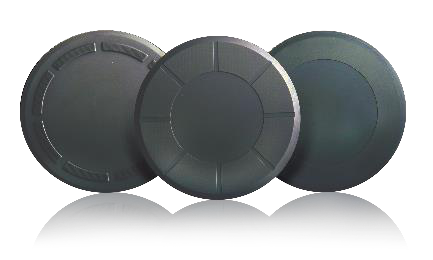
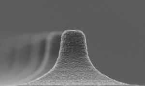
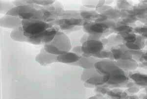
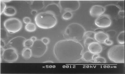
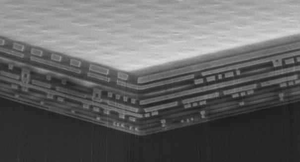
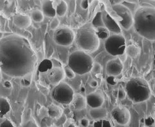
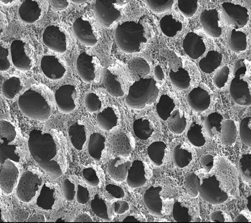
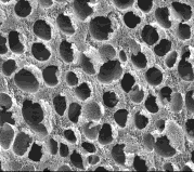
The material images show CMP slurry, a polishing pad and a multilayer wafer. The microscopic image labelled IC60 pad in the source illustrates its porous structure. Conditioning matched to the process maintains an effective pad surface and provides a basis for uniform wafer removal.


Restore the pad surface and stabilise removal
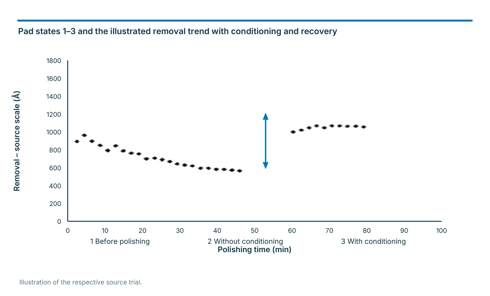
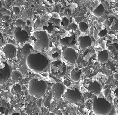
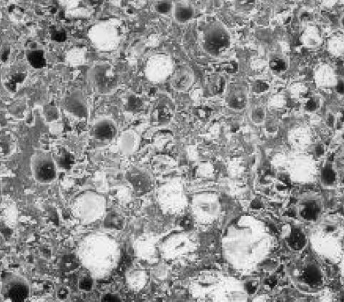
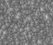
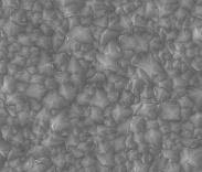
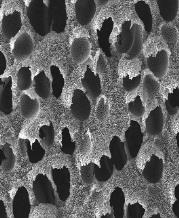
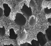
The pad surface changes during polishing. Without conditioning, pores and active surface structures can become loaded; the surface glazes and material removal decreases. The conditioner removes the altered upper pad layer and restores effective contact structures. The three microscopic images explicitly distinguish 1: before polishing, 2: polishing without conditioning and 3: polishing with conditioning.
The illustrated trend over 0–100 minutes shows a decline in removal followed by recovery through conditioning. The publication labels the vertical scale “Removal Rate (Å)”; it is used here to present this comparison.
Well-matched conditioning supports four connected process objectives: prevent pad glazing, control defects and topography, maintain high material removal and support wafer uniformity. These can contribute to longer pad life, a more stable CMP process and higher yield. Selection considers both the required surface activation and the pad consumption needed to achieve it.
The publications cite Y. Moon, Mechanical Aspects of the Material Removal Mechanism in Chemical Mechanical Polishing, UC Berkeley (1999), and S. H. Li and R. O. Miller, Chemical Mechanical Polishing in Silicon Processing, volume 63, pages 29–31, Academic Press (2000), as technical references.



Match the process variables
Diamond-tip design influences the conditioning action on the pad. Tip geometry, number, pattern and protrusion allow pad removal and roughness to be matched to the desired polishing result. PCR and wafer removal are different quantities. Higher PCR initially means more pad material removed; the resulting wafer removal also depends on pad, slurry, material and process settings.
Selection therefore considers activation, roughness, uniformity, defect behaviour and consumable cost together. The CVD and BSL comparisons illustrate these relationships using their respective metrics and test conditions.
| Metric | Meaning |
|---|---|
| PCR – Pad Cut Rate | Rate at which conditioning removes polishing-pad material |
| WRR – Wafer Removal Rate | Wafer removal rate |
| MRR – Material Removal Rate | Material removal rate; used for wafer removal in the CMP comparisons |
| Rpk | Reduced peak height of the roughness profile |
| CoC – Cost of Consumables | Consumable cost, expressed per wafer in the comparisons |
| POR – Process of Record | Reference process or reference tool for the respective comparison |
| AU | Relative or arbitrary units for the respective illustration |
CVD: engineered tips and effective contact areas
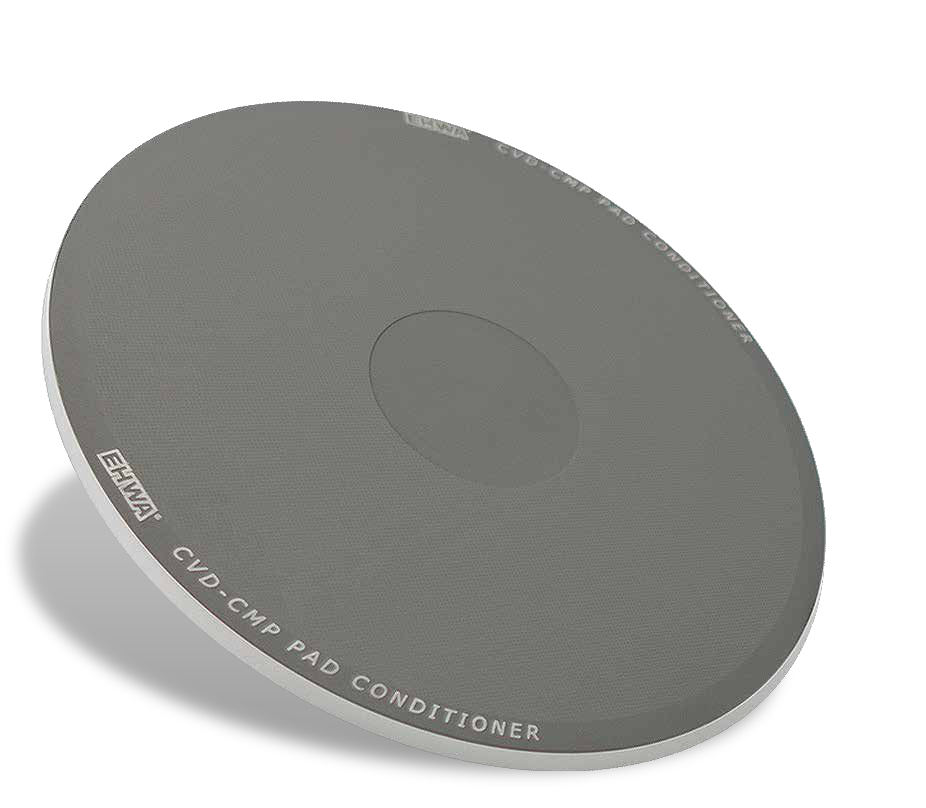
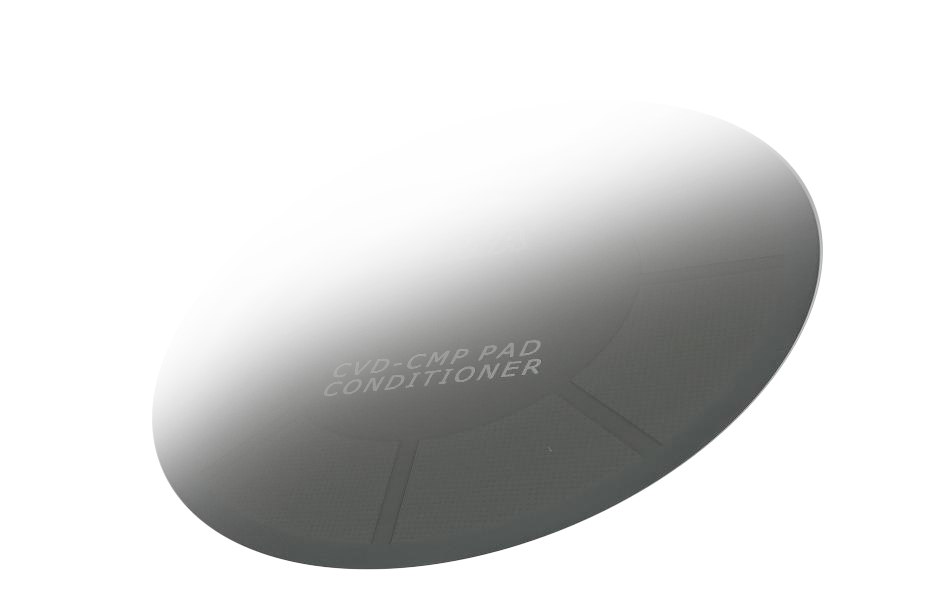
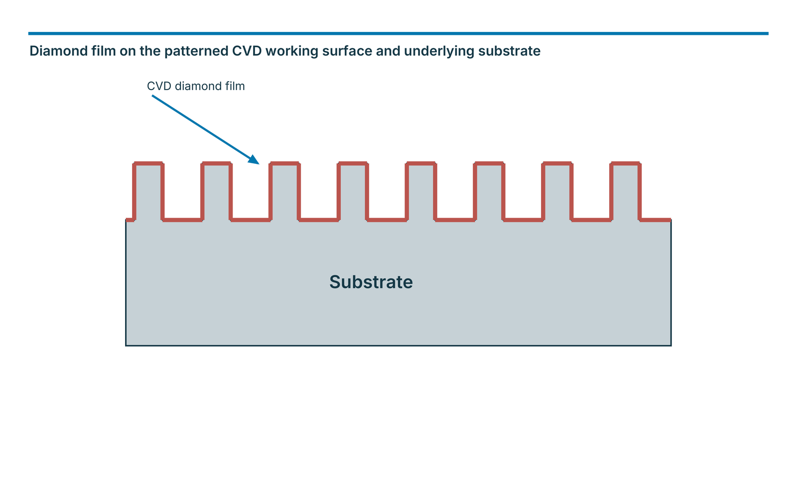
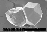
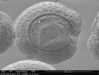
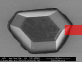
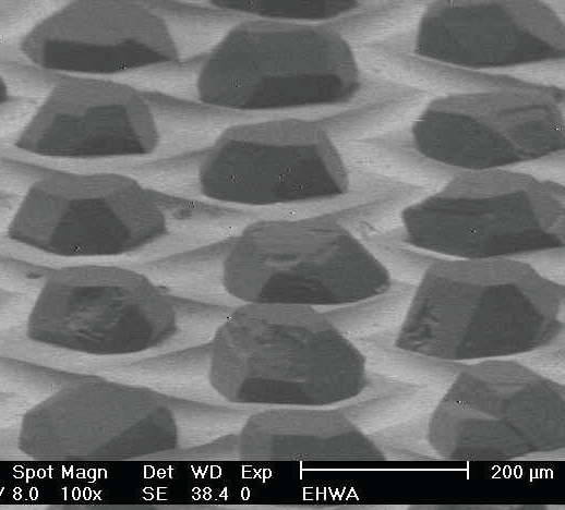
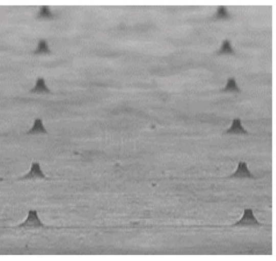
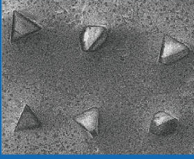
CVD conditioners use chemical vapor deposition to coat a patterned surface with diamond. This construction differs from individual diamond grains held by electroplated nickel or brazing. The tip pattern is engineered for the respective CMP process.
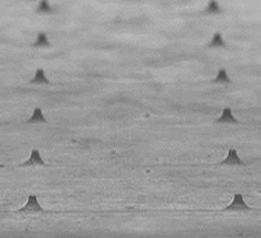
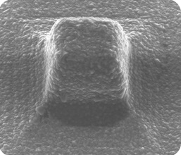
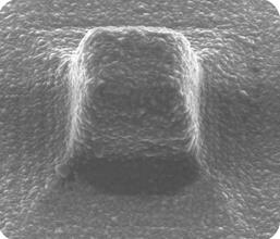
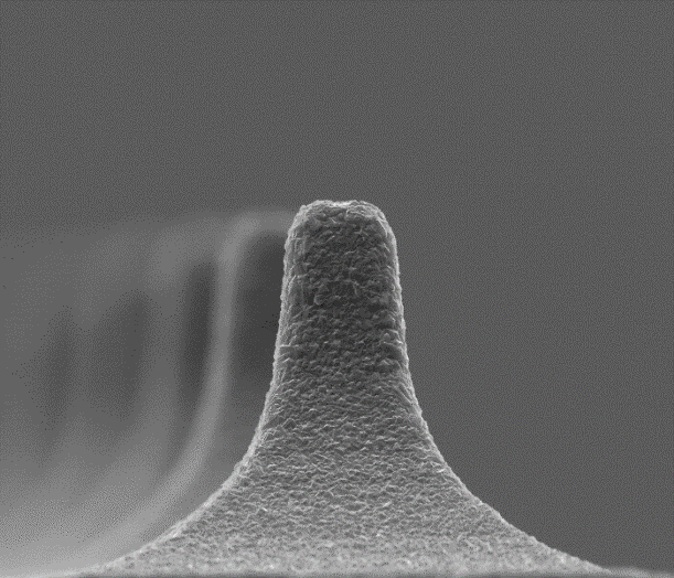
Uniform tip size and protrusion support flatness of the effective contact surface. A flat tip apex allows local loading to be engineered. Tip size, number, shape, pattern and protrusion influence PCR and wafer removal. In the illustrated conditioning concept, the engineered tip shape remains largely consistent over use, supporting stable contact conditions and conditioning action. EHWA also describes this development in its patent publications on tip and contact-area design.
The CVD surface provides high chemical stability. Its diamond-coated working surface can reduce exposure of metallic bonding material to process chemistry. The product sheets describe this benefit as avoiding corrosion and metal contamination. The selected disc is matched to the slurry actually used.
Customisation considers the polished material, pad and slurry. The application matrix lists oxide CMP with ceria-/silica-based slurry and tungsten and copper CMP, each with bulk and barrier steps. Closed-cell and open-pore pads are marked as application areas in all five process columns.
| Pad | Oxide CMP: ceria/silica | W CMP: bulk | W CMP: barrier | Cu CMP: bulk | Cu CMP: barrier |
|---|---|---|---|---|---|
| Closed-cell | ● | ● | ● | ● | ● |
| Open-pore | ● | ● | ● | ● | ● |




CVD and electroplated discs compared
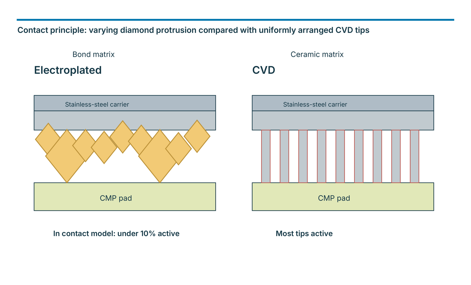
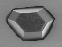
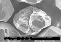
Diamond size and protrusion vary on the conventional electroplated disc. In the illustrated contact model, fewer than 10% of the grains act directly on the pad. The CVD disc has a diamond-coated patterned ceramic matrix; most uniformly arranged tips participate in contact. Both schematic carriers are labelled stainless steel.
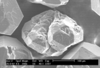
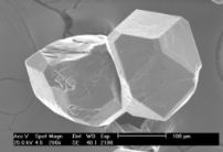
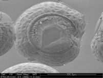
The comparison gives flatness greater than 20 µm for the conventional disc and less than 6 µm for the CVD disc. It also illustrates possible cracked grains, twin grains, crevice corrosion and diamond fallout in a nickel-based bond. The CVD ceramic tip shown is a continuous coated geometry, avoiding this mode of loss of individually bonded grains.
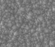
The corrosion comparison shows the CVD surface before immersion and after 320 hours in 10% hydrogen peroxide (H₂O₂). The illustrated images are described as showing no corrosion. This test applies to the surface and test solution shown. Engineered tips combined with chemical resistance support uniform conditioning with reduced risk from bond corrosion.
| Comparison feature | Conventional electroplated | CVD |
|---|---|---|
| Carrier in schematic | Stainless steel | Stainless steel |
| Working structure | Diamond grains in bond matrix | Diamond-coated patterned ceramic matrix |
| Active contacts in model | <10% of diamond grains | Most tips |
| Flatness | >20 µm | <6 µm |
| Illustrated breakage risk | Cracked and twin diamonds; nickel-based metal bond | Coated ceramic tip |
| Illustrated corrosion behaviour | Crevice corrosion and diamond fallout | No corrosion reported after 320 h in 10% H₂O₂ |

CVD product ranges and customisation
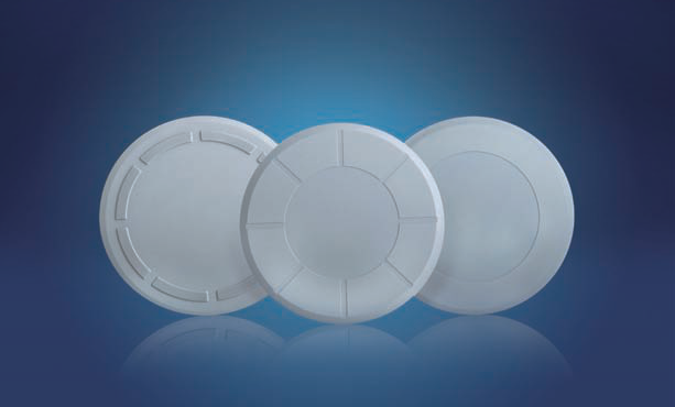
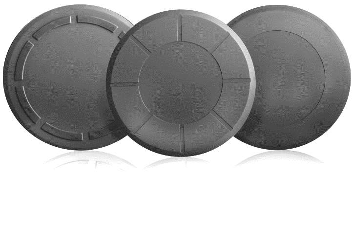
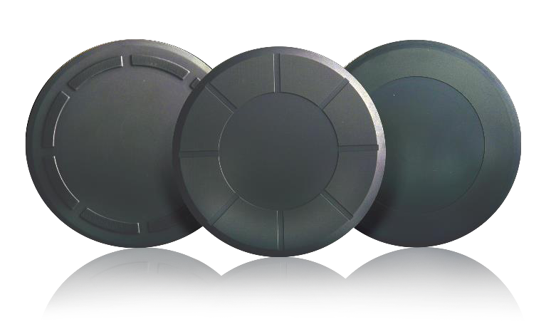
The CVD product sheets specify an outside diameter of 2–5 inches. Tip size, number and height are customised within the stated ranges. Height is determined according to tip size. These specifications belong to the programme described in the product sheets and provide a basis for application engineering.
A flat apex and engineered tip pattern allow the effective contact area to be tailored. The resulting load per tip is an important design variable. The objective is a sufficiently active pad surface with consistent roughness and economical pad consumption.
| Feature | Range stated in product sheet |
|---|---|
| Outside diameter | 2–5 inches |
| Tip size | Customised, over 5 µm |
| Tip number | Customised, below 30,000 per disc |
| Tip height | Customised, below 100 µm; determined by tip size |
Consistent conditioning through pad use
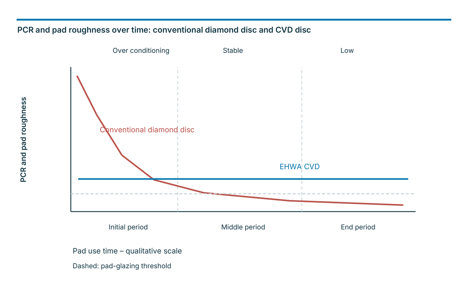
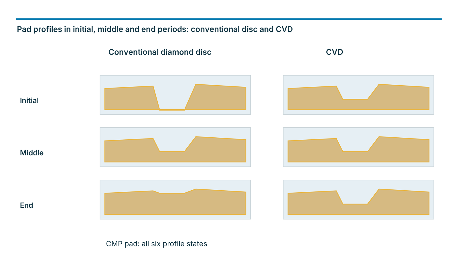
The product sheets compare a conventional diamond disc and a CVD disc over time. In the conventional design, PCR and pad roughness decline considerably in the illustrated trend: strong initial conditioning is followed by a stable middle period and finally low conditioning action. The CVD line remains above the indicated pad-glazing threshold in the model.
The six corresponding pad profiles illustrate the different action in initial, middle and end periods. The conventional profile changes from a deep cut to a shallower contact profile; the CVD profiles remain similar across the three stages. The diagrams describe a qualitative comparison without numerical time or roughness values.
Uniform tip shape and contact area support process stability over use. Controlled conditioning aims to limit both excessive initial pad cutting and insufficient activation towards the end. This can extend the period during which a disc operates within a suitable working range.
Pad life, wafer removal and consumable cost
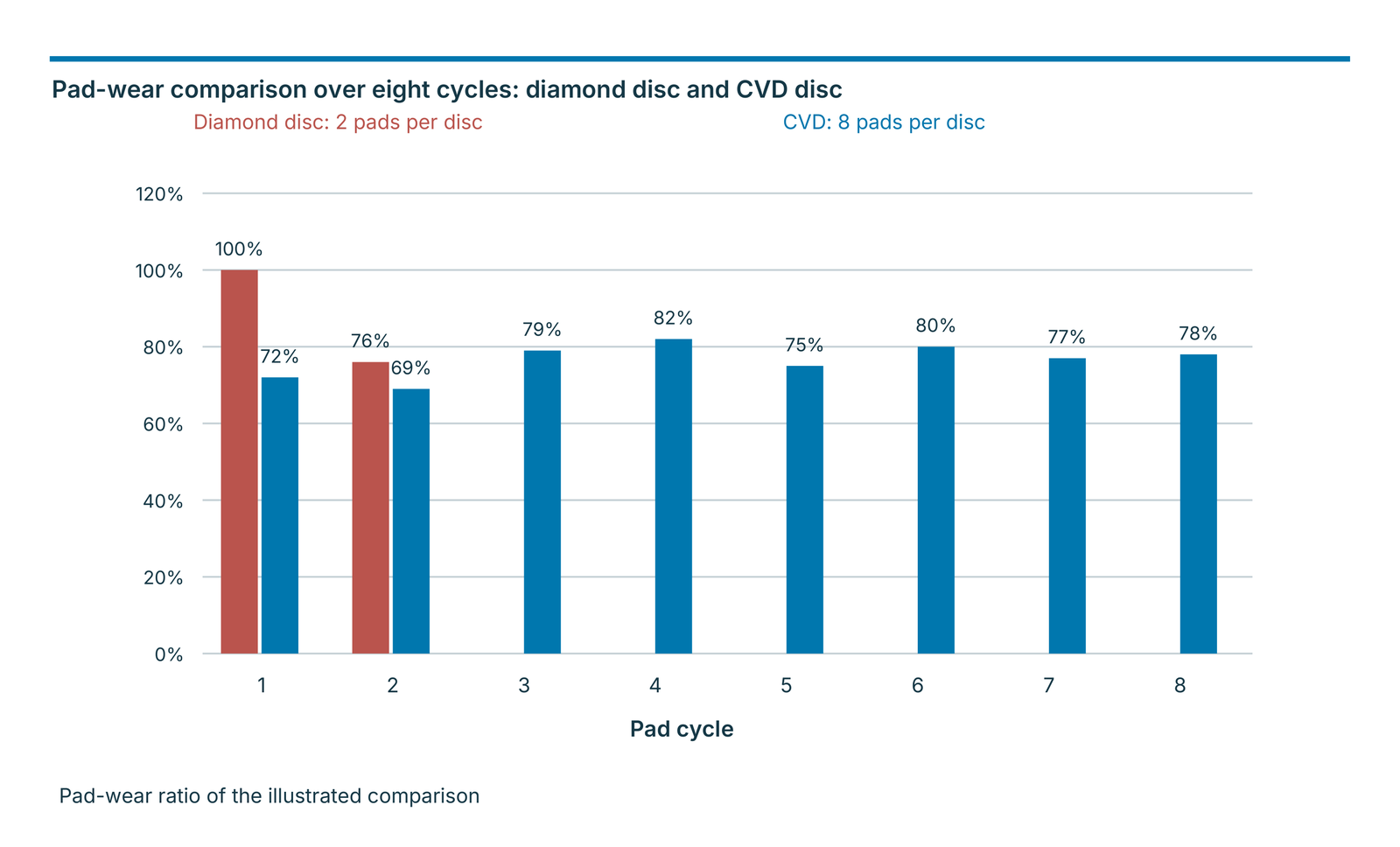
A consistent diamond-tip contact area supports stable wafer removal. Low but sufficient pad wear can extend pad life. If one conditioning disc can be used with several pads, consumable cost per wafer can also decrease.
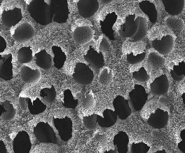
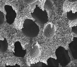
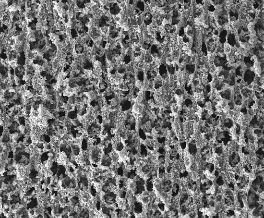
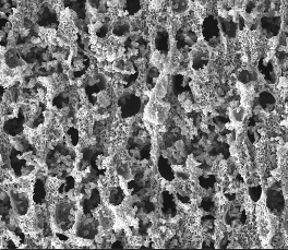
The specific pad-wear comparison describes two pads per conventional diamond disc and eight pads per CVD disc. The percentage values for all eight cycles are listed in the table. Microscopic images compare a new pad, POR after 40 hours or one cycle, and CVD after one and six cycles, each at 100× and 200× magnification.
A second trend plots normalised wafer removal over 0–50 hours of pad use: POR covers one cycle and CVD two cycles. The illustrated CVD curve remains approximately stable over a longer usage range. These comparisons refer to the pad and process examples shown and illustrate the benefit of limited diamond wear and matched conditioning.
| Cycle | Diamond disc: pad-wear ratio | CVD: pad-wear ratio |
|---|---|---|
| 1 | 100 % | 72 % |
| 2 | 76 % | 69 % |
| 3 | — | 79 % |
| 4 | — | 82 % |
| 5 | — | 75 % |
| 6 | — | 80 % |
| 7 | — | 77 % |
| 8 | — | 78 % |



Pad debris, contact pressure and defect control
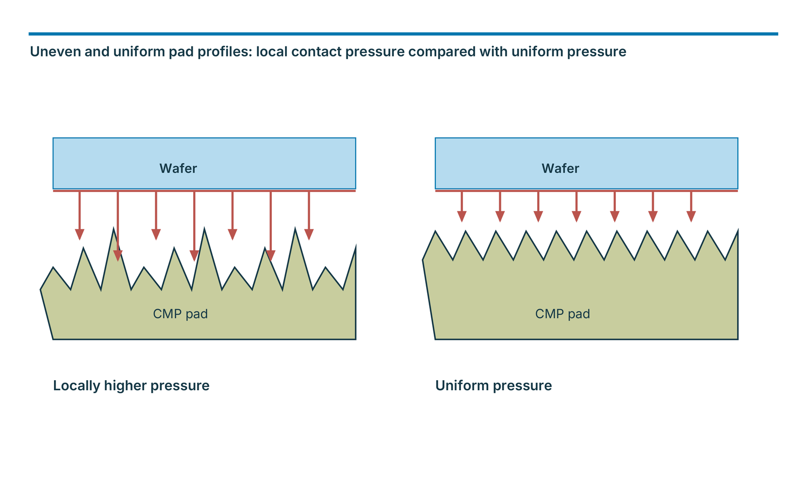
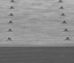
Large pad-debris particles can cause wafer defects. Flat CVD tips with uniform height limit pronounced individual contacts and support control of these particles. Controlled pad debris and lower pad roughness provide favourable conditions for defect and topography control.
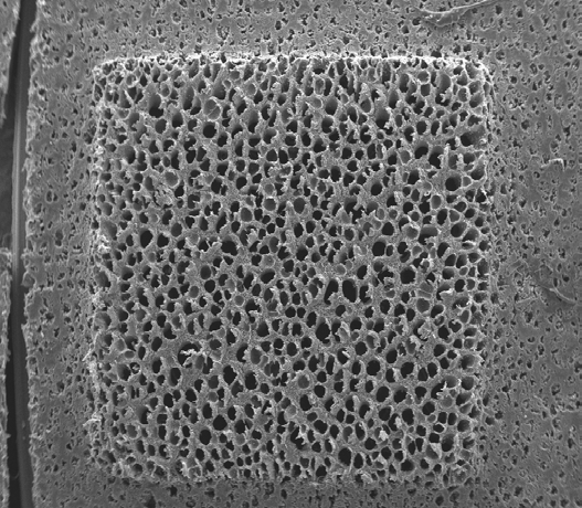
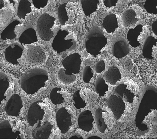
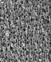
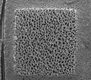
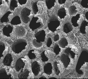
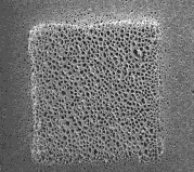
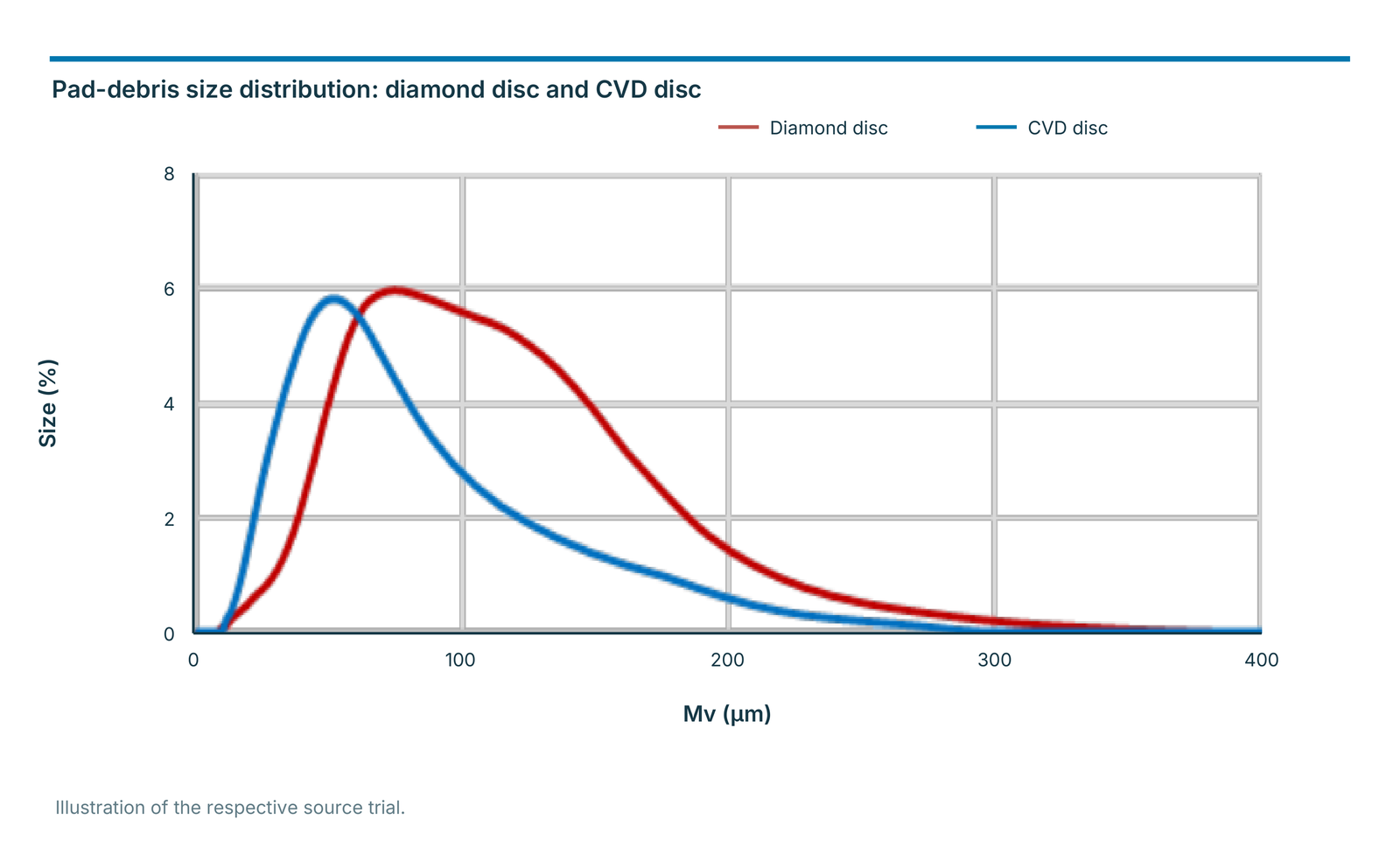
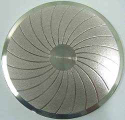
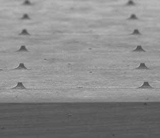
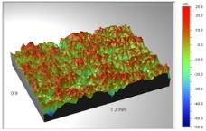
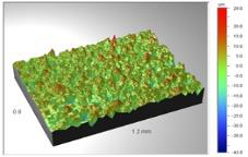
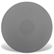
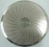
The contact illustrations distinguish locally higher, non-uniform pressure from more uniform pressure distribution. The corresponding surface measurements show the respective pad textures. The particle-size-distribution diagram compares a conventional diamond disc and a CVD disc using the original “Size %” and “Mv (µm)” scales.
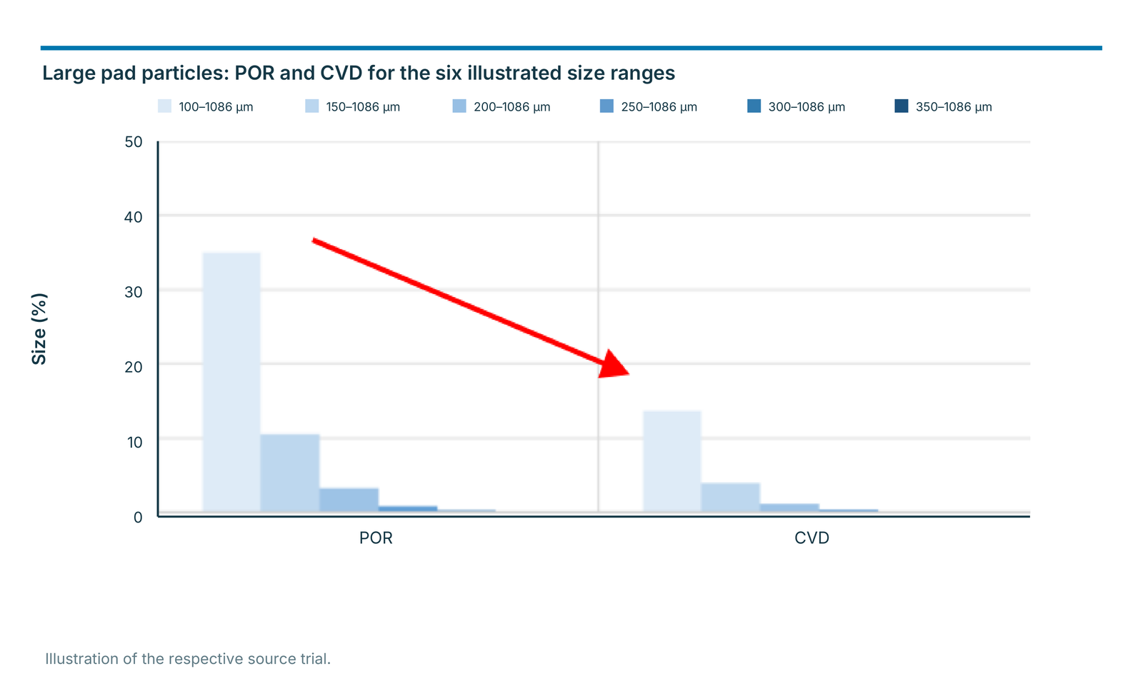
The second comparison presents larger particles for POR and CVD. The six ranges start at 100, 150, 200, 250, 300 and 350 µm respectively and all end at 1086 µm. These ranges overlap, so their bars are not added to form a total. The illustrated CVD comparison shows lower proportions of large particles. Both diagrams describe their respective trials and support selection of an appropriate tip pattern.
Limit dishing and erosion over pad life
Uniform tip height can create a smoother and more consistent pad surface. Low, stable pad roughness supports limiting dishing and erosion throughout pad use. Tip configuration is selected to achieve the desired surface action.
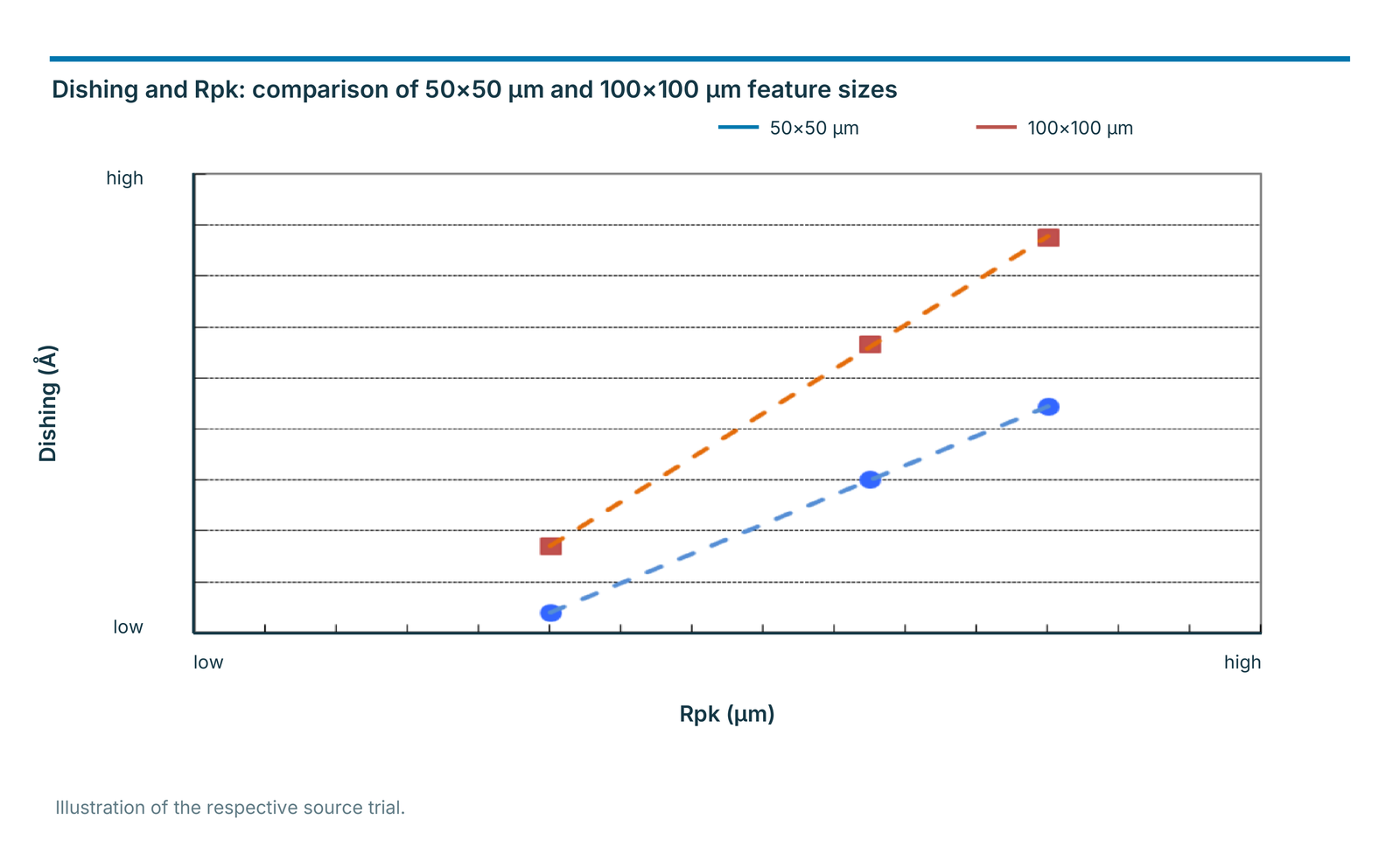
The application example plots dishing against Rpk and distinguishes 50×50 µm and 100×100 µm features. Both series rise with increasing Rpk; the larger feature shows a stronger increase in dishing within the illustrated range. The axes carry Å and µm units but use only low and high scale labels. The table lists all stated process conditions.
The publications use “Near-zero” to describe low variation in tip height. The specific flatness figure in the comparison remains <6 µm. Engineered tips, low pad roughness and extended disc use link process quality to the objective of lower consumable costs.
| Parameter | Condition |
|---|---|
| Polisher | AMAT Reflexion LK |
| Wafer | Cu patterned wafer |
| Slurry | Cu slurry |
| Conditioner | CVD disc |
| Compared feature sizes | 50×50 µm; 100×100 µm |
BSL: strong grain retention and useful diamond protrusion
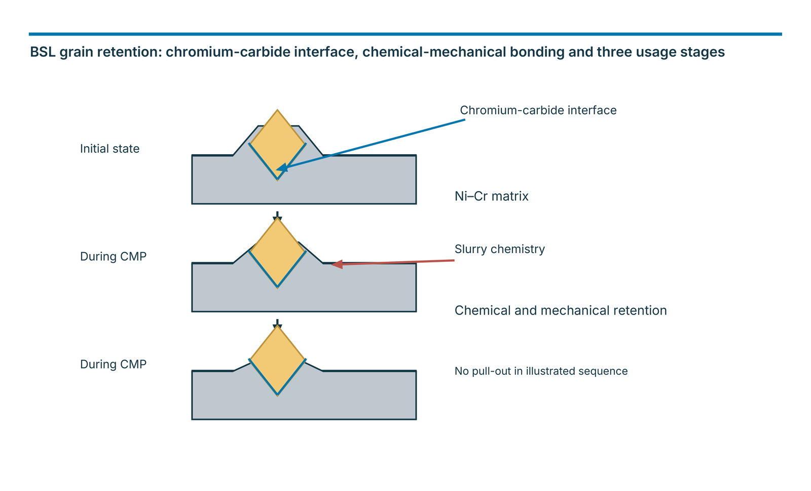
BSL conditioners combine mechanical retention with chemical bonding between diamond and metal matrix. The brazing process uses EHWA-developed brazing powder and high-temperature/vacuum processing. A carbide layer forms at the interface, supporting grain retention and resistance to process chemistry.
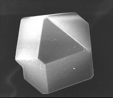
Diamond orientation uses faces and edges for conditioning. High protrusion provides larger spaces for pad debris, supporting efficient pad cutting and debris removal. The combination of brazed bonding and diamond orientation targets high PCR and pad roughness maintained over extended use.
A long-lasting disc can enable longer pad life, fewer pad changes and higher equipment uptime, helping control CMP consumable costs. The publications also identify BSL as a technology for high material removal in SiC CMP and describe use as a POR conditioner in reference processes. The particular SiC slurry and intended process determine the design.
Chemical-mechanical bonding and electroplated nickel bonding
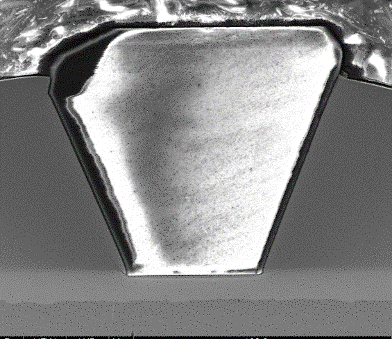
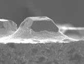
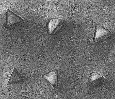
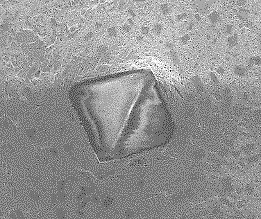
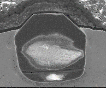
The BSL illustration shows diamond in a nickel–chromium matrix. Chemical reaction forms chromium carbide at the interface, while the matrix also mechanically surrounds part of the diamond. The cross-section shows close interfacial contact without the gap indicated in the comparison.
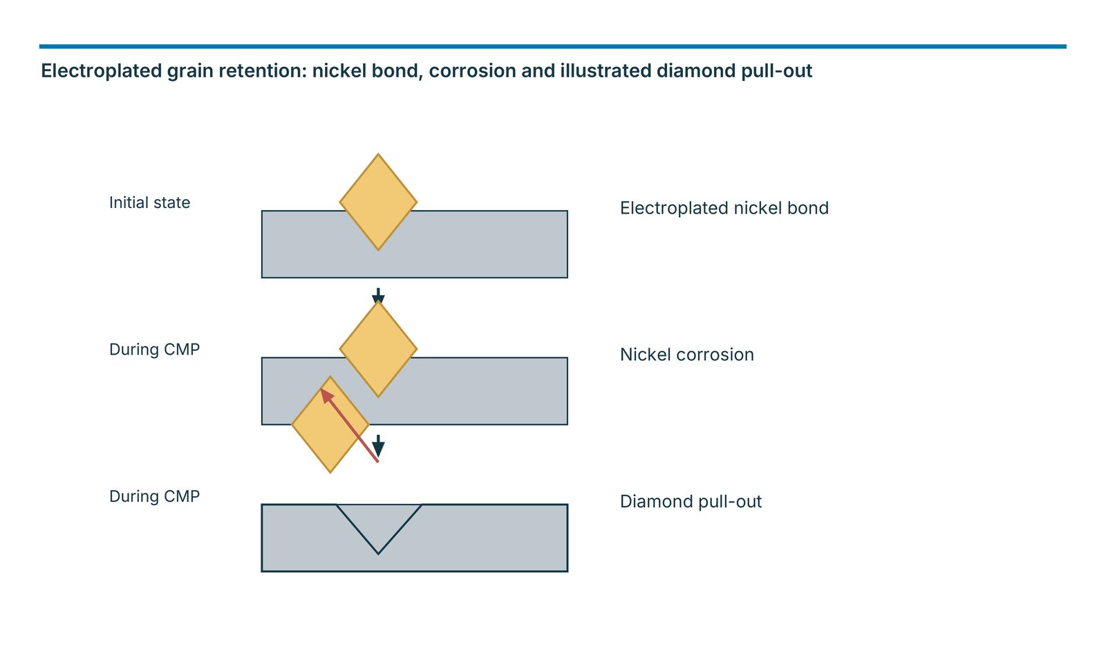
The electroplated design mechanically retains diamond within the surrounding nickel layer. Its schematic usage sequence shows nickel corrosion followed by diamond pull-out. The corresponding cross-section marks an interface gap. Both bonding concepts are illustrated with initial images and images after the stated usage.
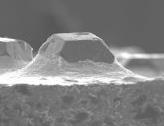
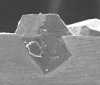
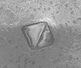
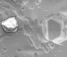
No diamond loss is reported for the BSL disc after 60 hours of use; substantial loss is shown for the electroplated comparison disc after 20 hours. These observations of different duration belong to the respective discs shown. They demonstrate the illustrated retention advantage without establishing a fixed tool-life multiplier. The images and process stages show how chemical bonding and mechanical retention together support reliable conditioning.
| Feature | BSL | Electroplated |
|---|---|---|
| Bonding principle | Chemical and mechanical retention | Mechanical retention by nickel |
| Interface in example | Chromium carbide; close contact without indicated gap | Marked interface gap |
| Usage shown | 60 h | 20 h |
| Observation in example | No diamond loss reported | Substantial diamond loss shown |
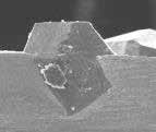
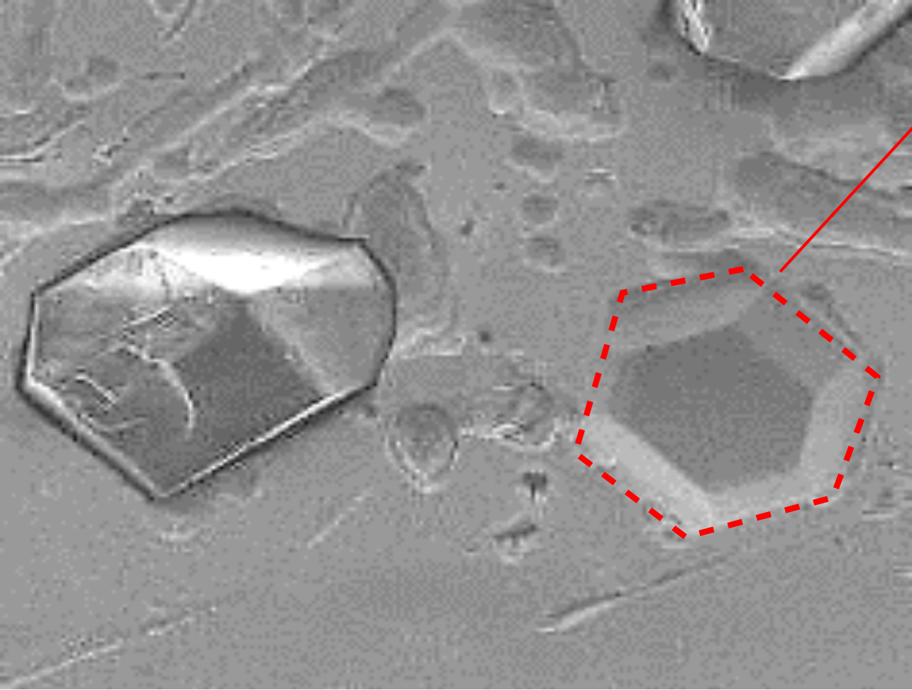
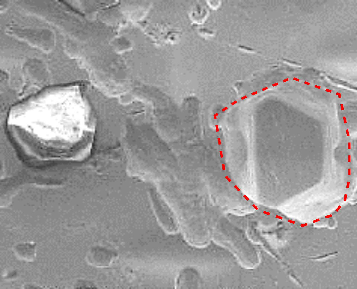
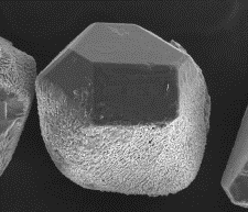

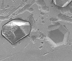
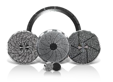
Grain-retention test on an aluminium platen
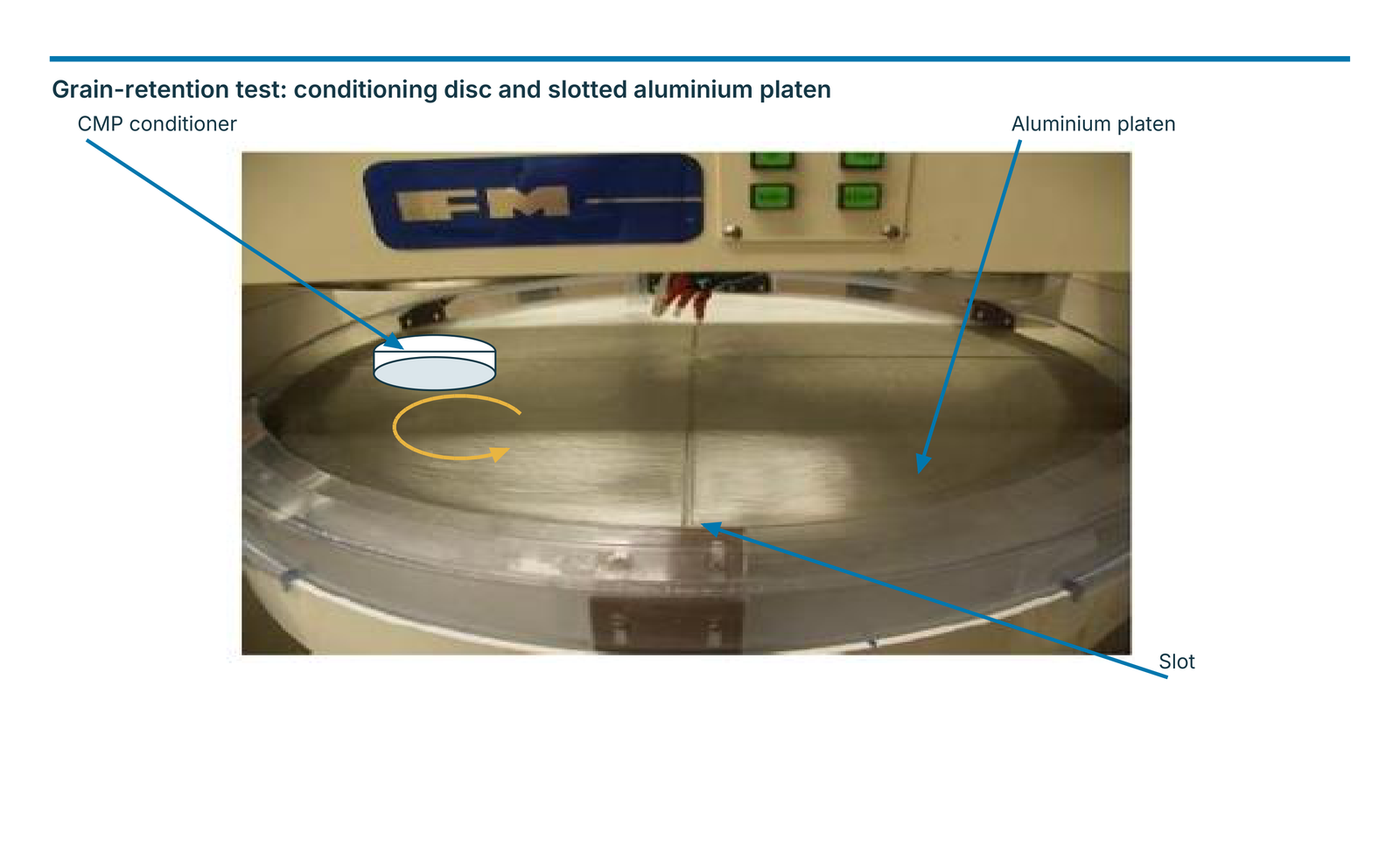
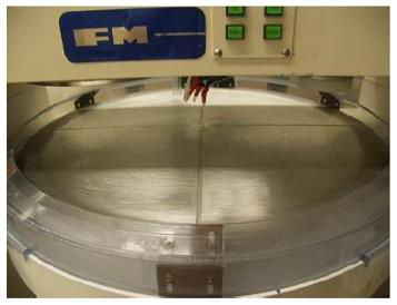
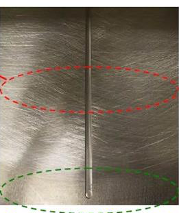
A separate test assesses diamond retention by conditioning an aluminium platen with a slot. The interrupted contact is intended to dislodge diamonds from the conditioning disc, creating a targeted comparison of bond strength. Photographs show the setup and identify conditioned and unconditioned regions on the aluminium surface.
The comparison uses a sintered disc from company A, a brazed disc from company B and an EHWA BSL disc. Diamond losses for the stated 5- and 30-minute test intervals are listed in the table. No diamond pull-out is observed for EHWA BSL in this test. This retention test is separate from the CMP usage images after 60 and 20 hours.
| Disc type | After 5 min | After 30 min | Total diamond pull-out |
|---|---|---|---|
| Company A: sintered | 2 | 2 | 4 |
| Company B: brazed | 2 | 3 | 5 |
| EHWA BSL | 0 | 0 | 0 |
Diamond protrusion and pad removal
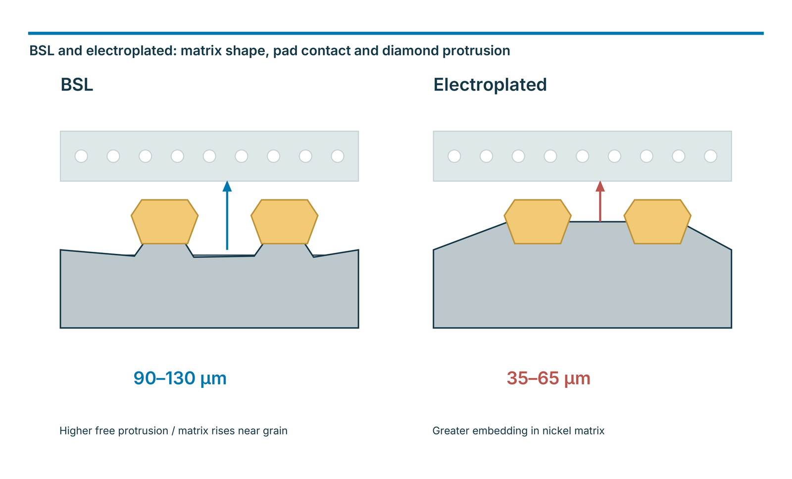
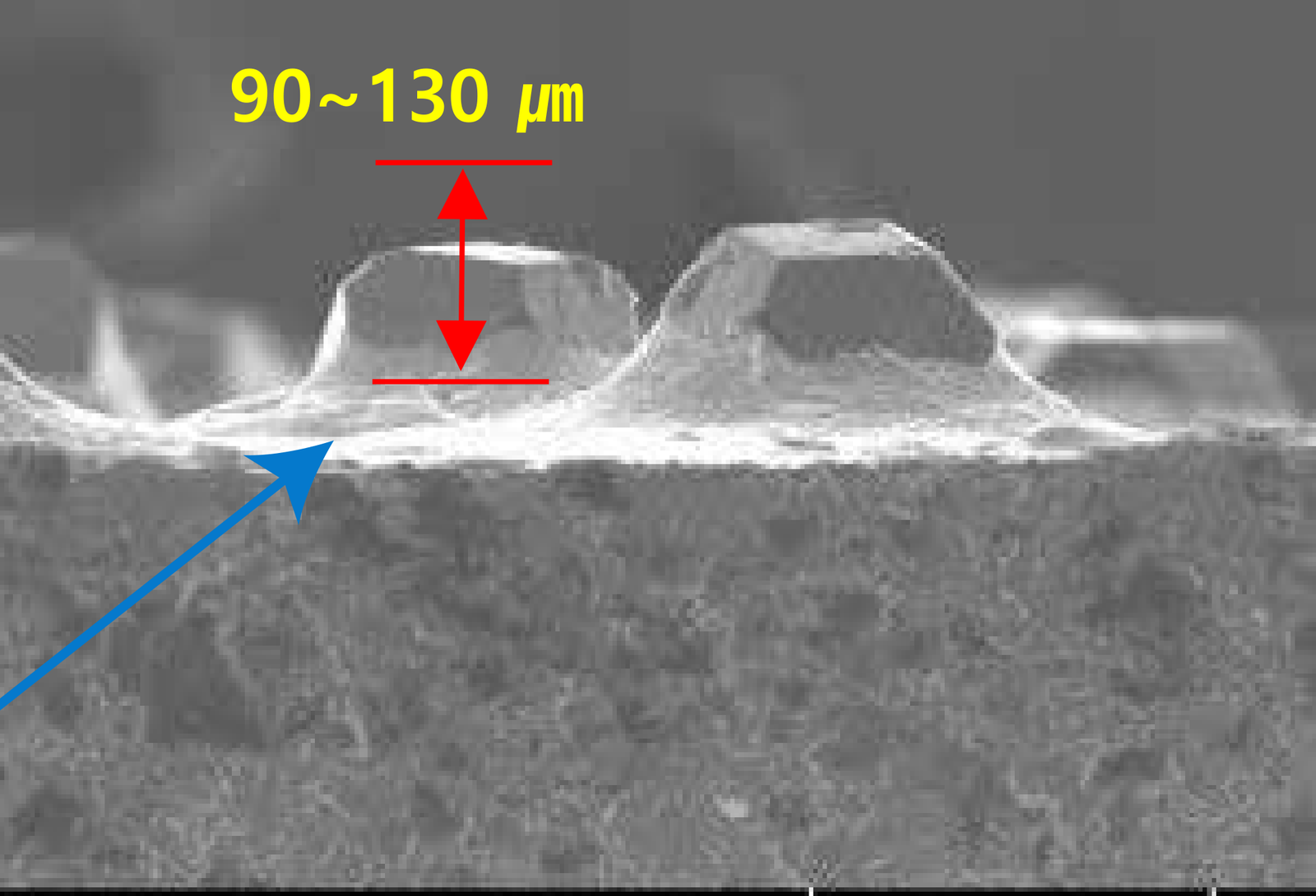
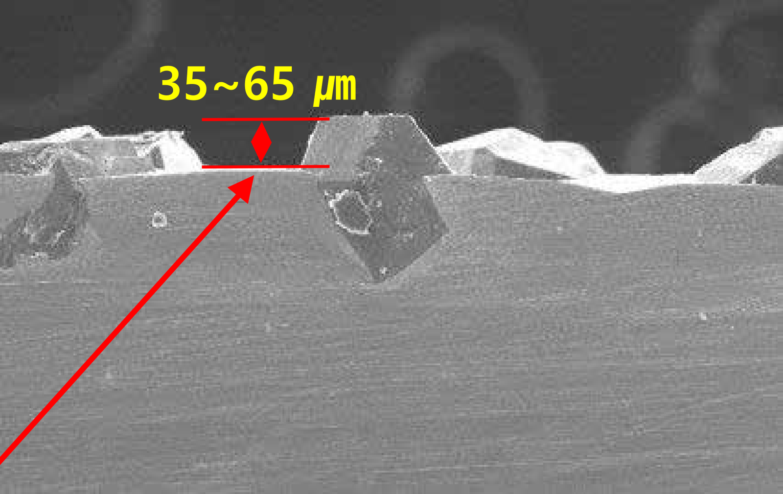
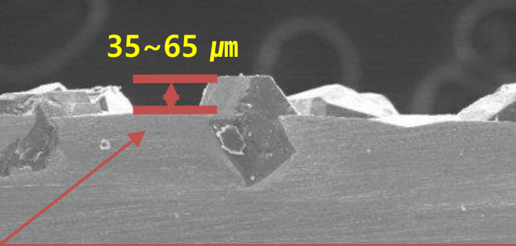
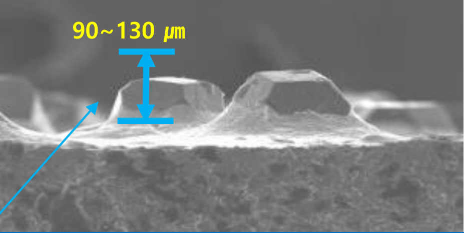
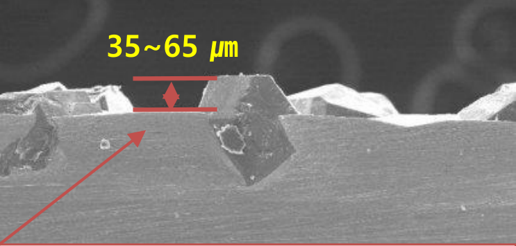
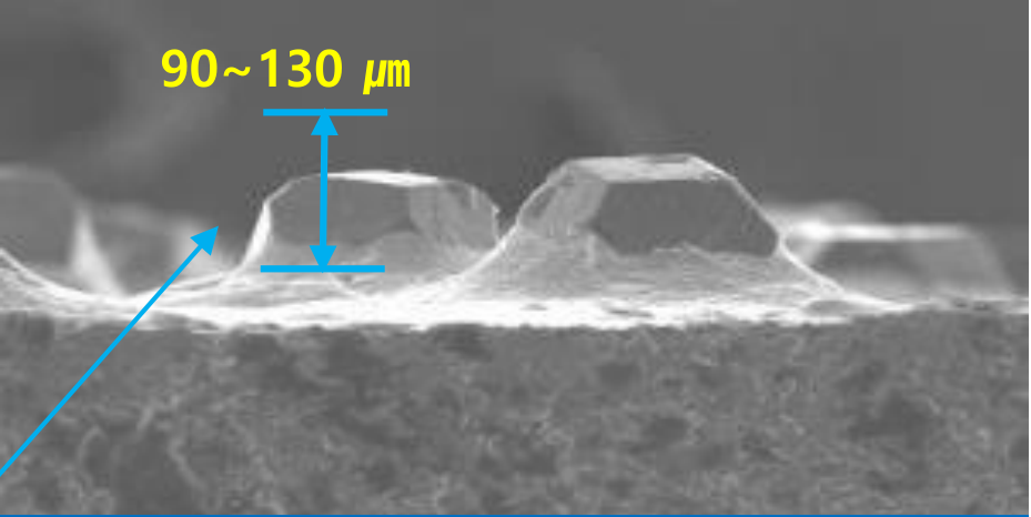
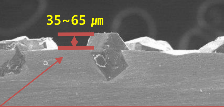
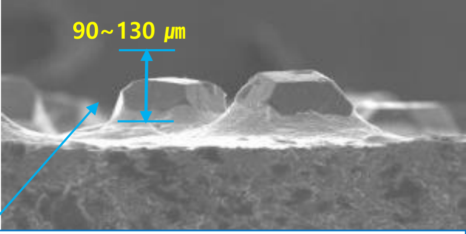
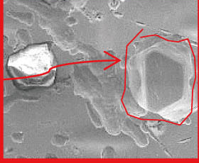
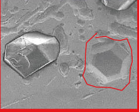
In the BSL concept, the metal matrix rises mainly immediately around each diamond, leaving more space between grains. The electroplated nickel matrix surrounds more of the grain to provide mechanical retention. The illustrated protrusions are 90–130 µm for BSL and 35–65 µm for the electroplated design.
The comparison plots PCR in percent for diamond types A to E. BSL is higher than the electroplated comparison disc in all five pairs shown; both series decrease from A to E. The different protrusions and open spaces explain the higher pad cut rate in the illustrated example.
Higher protrusion can support efficient conditioning and the required pad activation. Its effect on wafer removal is matched to pad and slurry: the higher PCR in this BSL comparison is a different metric from wafer material removal.
| Design | Illustrated diamond protrusion |
|---|---|
| BSL | 90–130 µm |
| Electroplated | 35–65 µm |

Maintain suitable pad roughness for longer
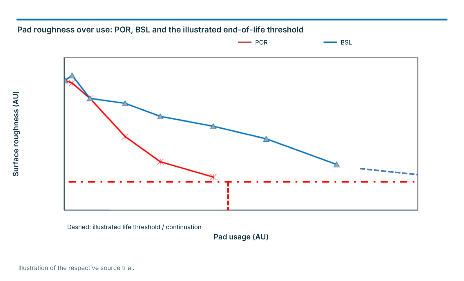
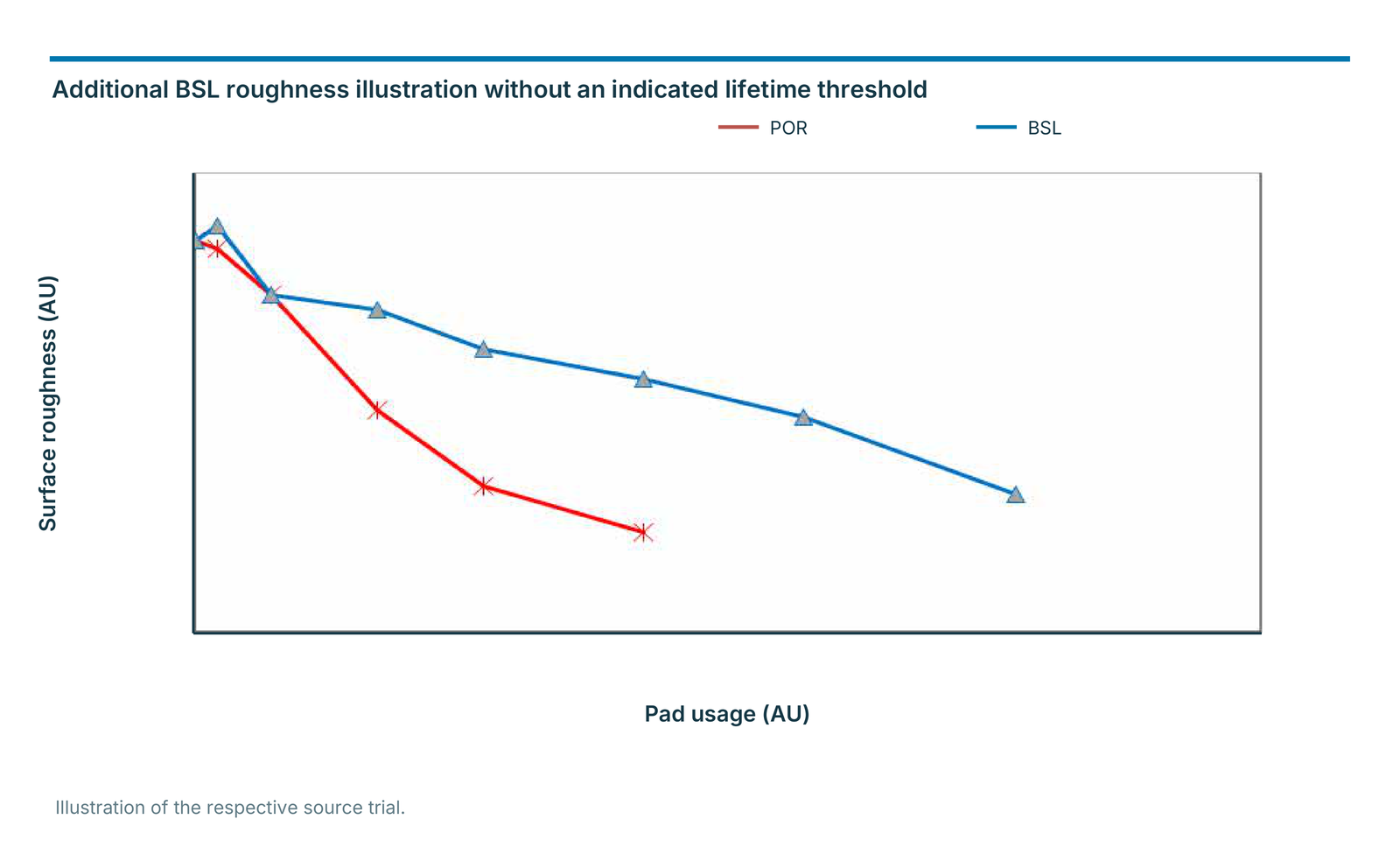
Brazed bonding and controlled diamond orientation support conditioning that remains effective over extended use. The illustrated roughness trends compare BSL with a POR reference process. The POR curve declines faster in the model, while BSL maintains higher surface roughness over a longer usage range.
One variant marks the lower roughness threshold and the end of pad life for the POR example. The BSL curve continues beyond it as a dashed line. Another illustration shows both trends without a lifetime threshold. Both axes are expressed in AU; these qualitative scales do not establish a fixed life in hours.
The benefit is suitable contact conditions for longer and fewer pad changes. A long-lasting conditioner can therefore support higher equipment uptime and lower consumable cost.
BSL double-layer and electroplated variants: applications and product data
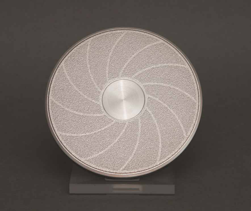
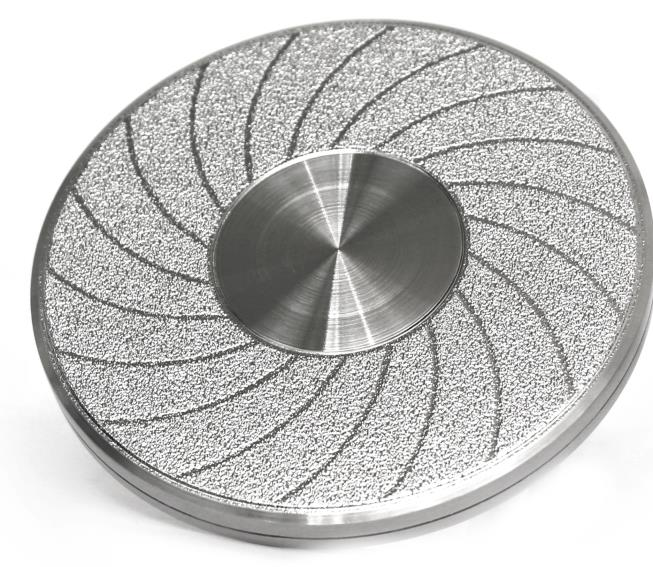
The product sheets list a new BSL design with a double metal layer and an electroplated design. The application overview covers oxide CMP with BPSG, TEOS and PSG; metal CMP with aluminium, tungsten and copper; and STI, PGI, poly-Si and TSV CMP with Cu or poly-Si. PGI and the material/process designations are retained as given in the publication.
The programme names AMAT, Ebara, Novellus, Strasbaugh and Lam models. The stated pad cut rate range is 10–300 µm/h. Machine names and the product range come from the product sheets; the required design is selected for the equipment and process.
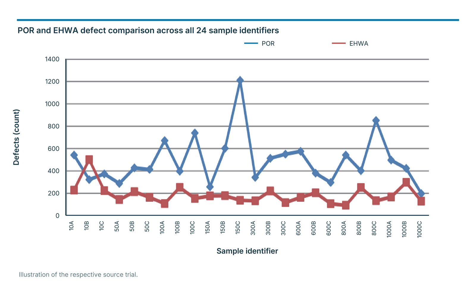
The defect comparison plots POR and EHWA across 24 identifiers from 10A to 1000C. All identifiers, points and the count scale are retained. The EHWA series is lower in most comparisons shown; the source does not provide complete process conditions for this dataset. The example illustrates the intended defect control and remains separate from the other retention and pad-life trials.
| Application group | Named materials / processes |
|---|---|
| Designs | New BSL double metal layer; electroplated design |
| Oxide CMP | BPSG, TEOS, PSG |
| Metal CMP | Al, W, Cu |
| Further processes | STI, PGI, poly-Si; TSV CMP → Cu, poly-Si |
| Manufacturer | Models listed in product sheet |
|---|---|
| AMAT | Mirra / Reflexion |
| Ebara | F-Rex200/300; EPO-222(H) |
| Novellus | Auriga; CMP200/300; Avantgaard 776 (676); Momentum |
| Strasbaugh | 6DS-SP; 6ED |
| Lam | Teres |
| Pad cut rate of the described programme | 10–300 µm/h |

Large-format conditioners: bars, rings and pellets
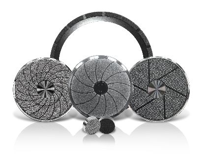
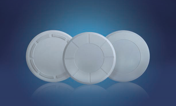
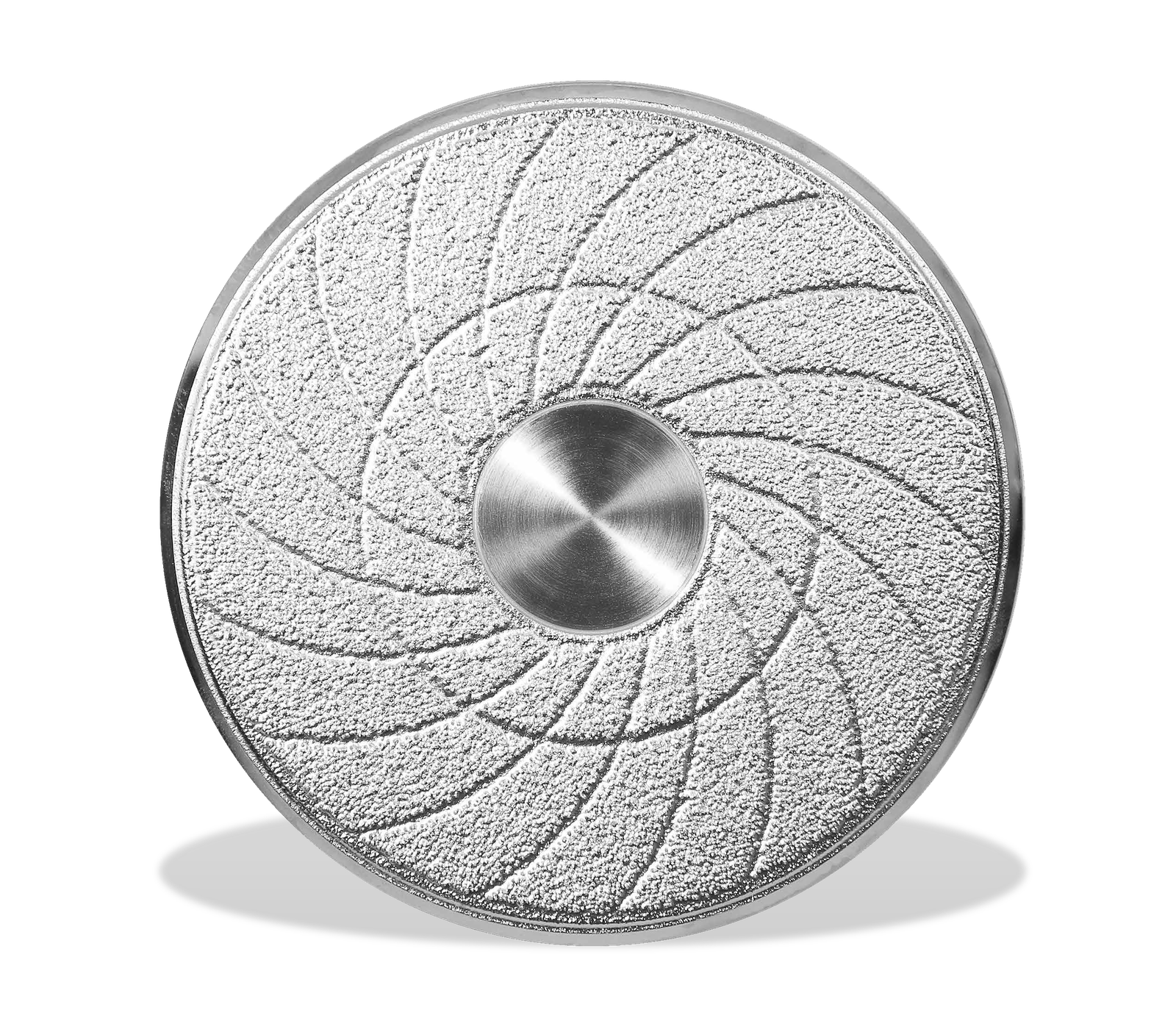
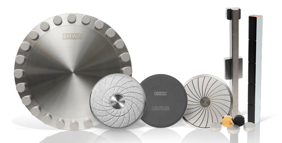
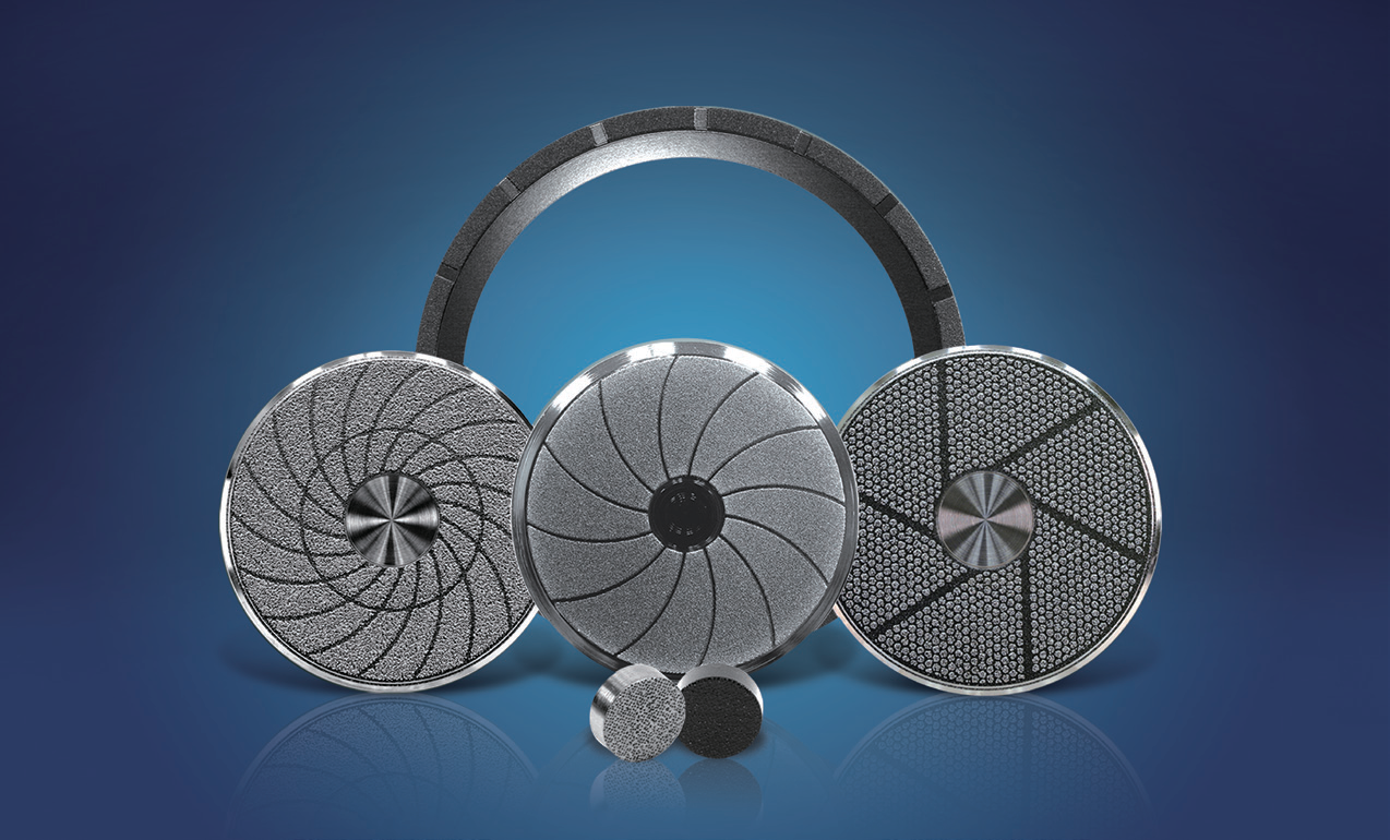
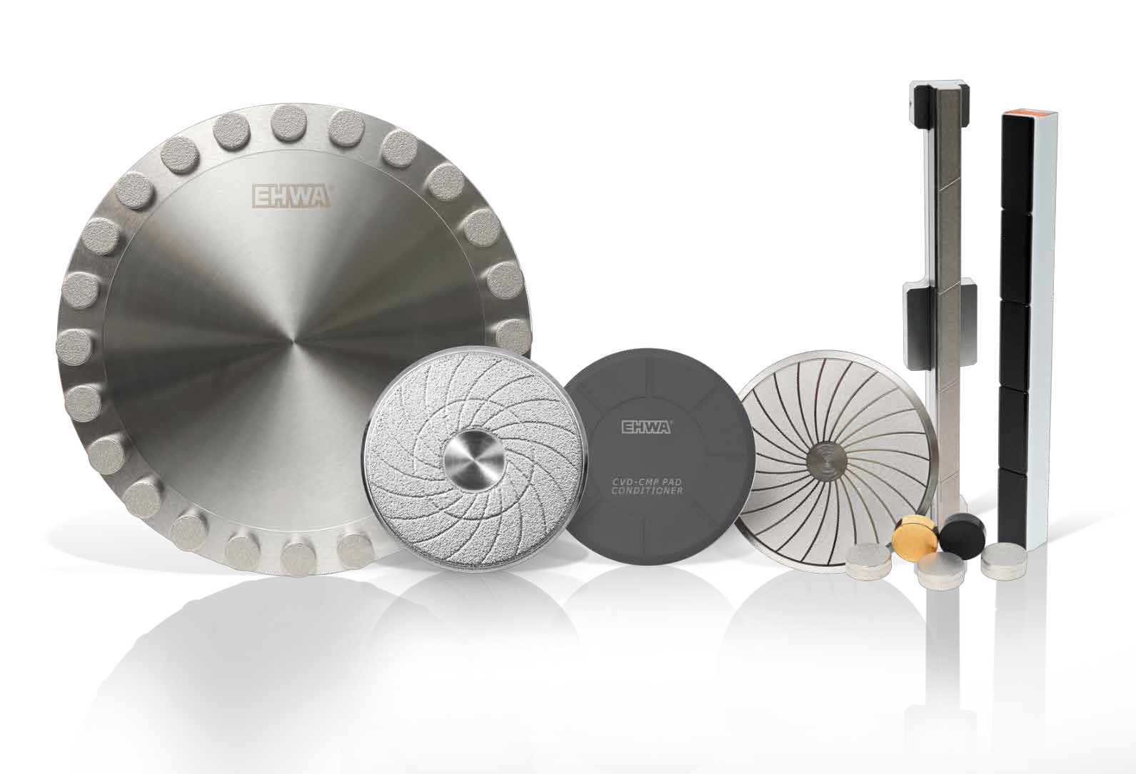
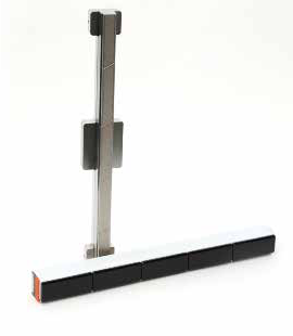
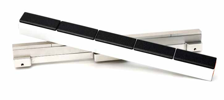
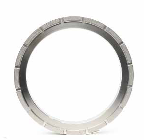
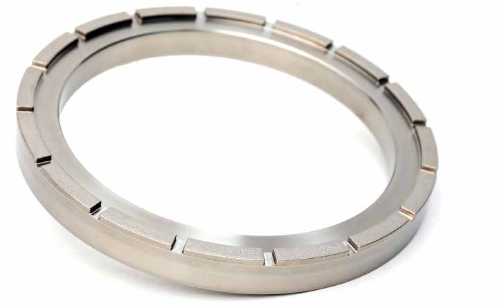
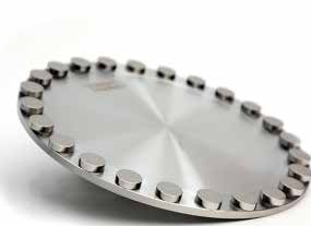
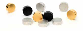
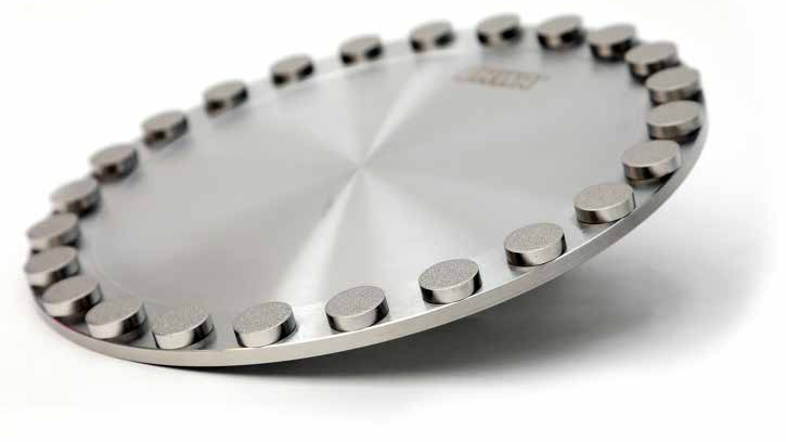
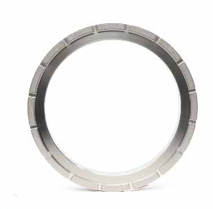
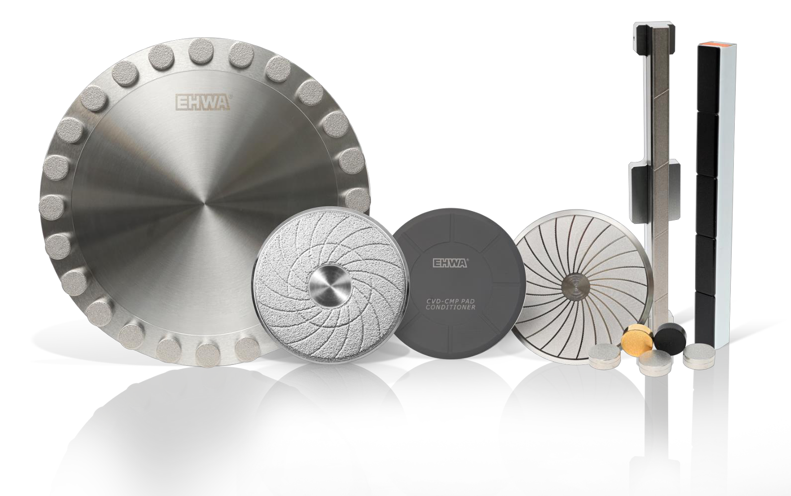
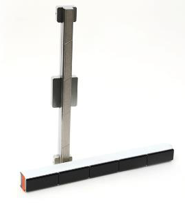
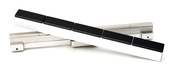
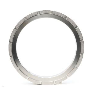
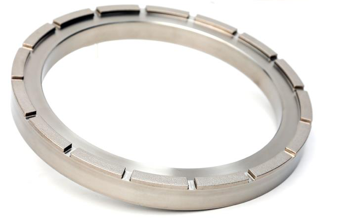
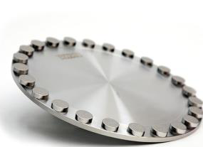
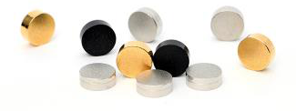
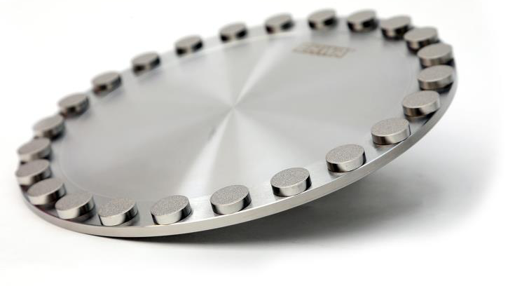
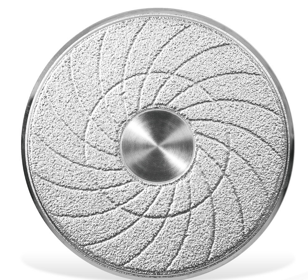
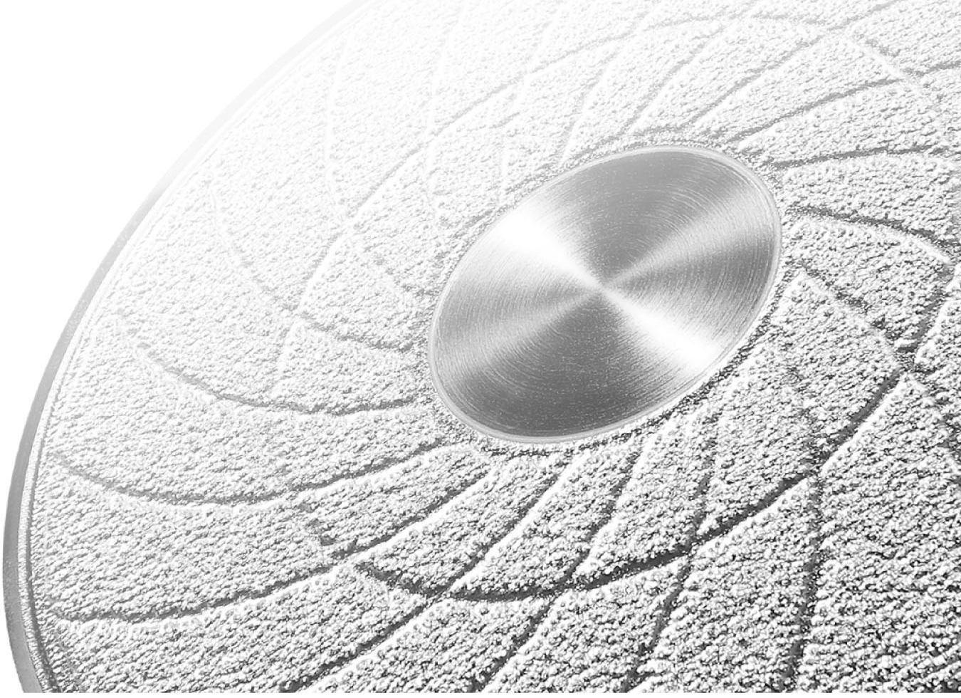
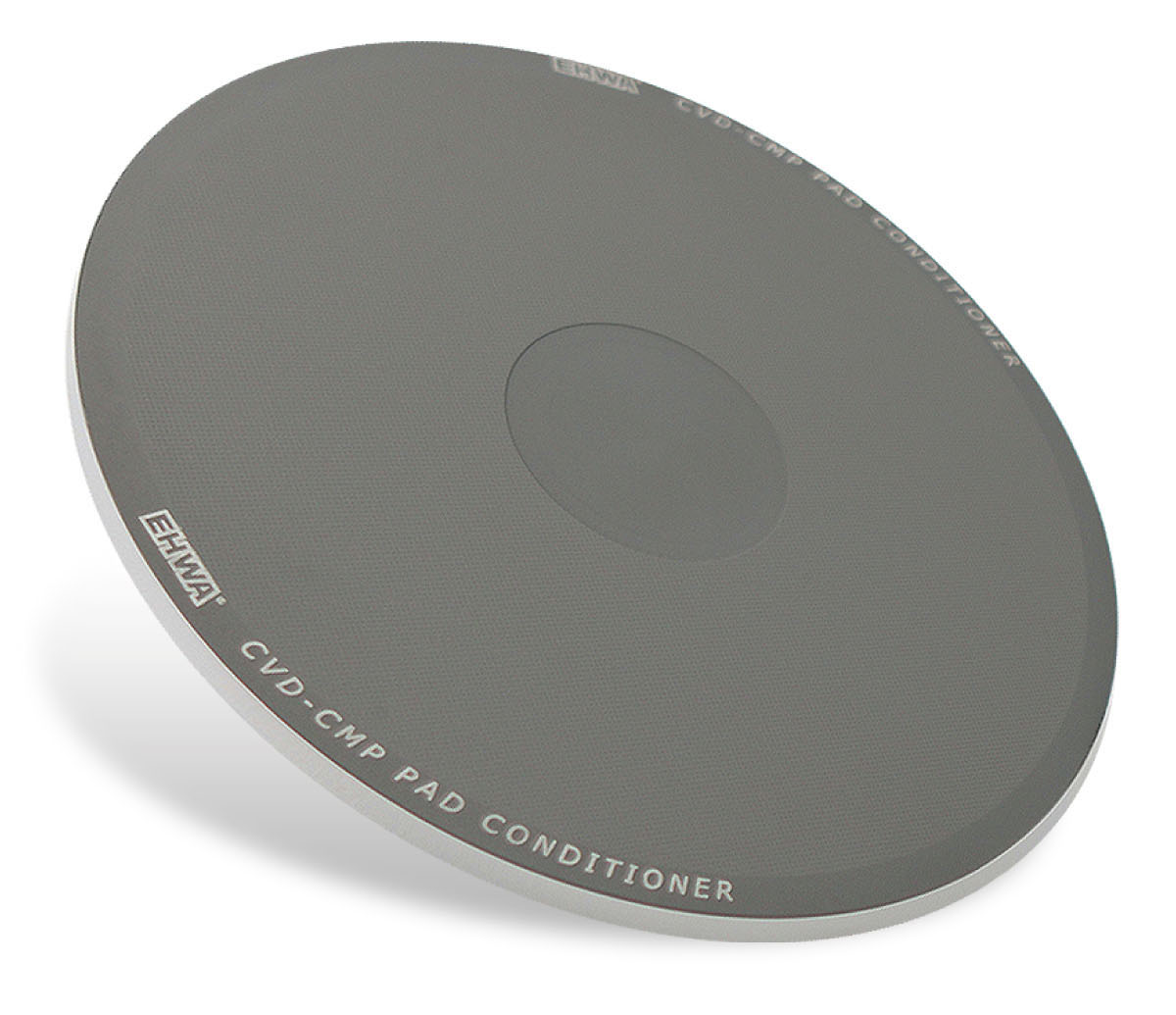
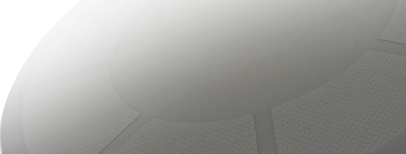
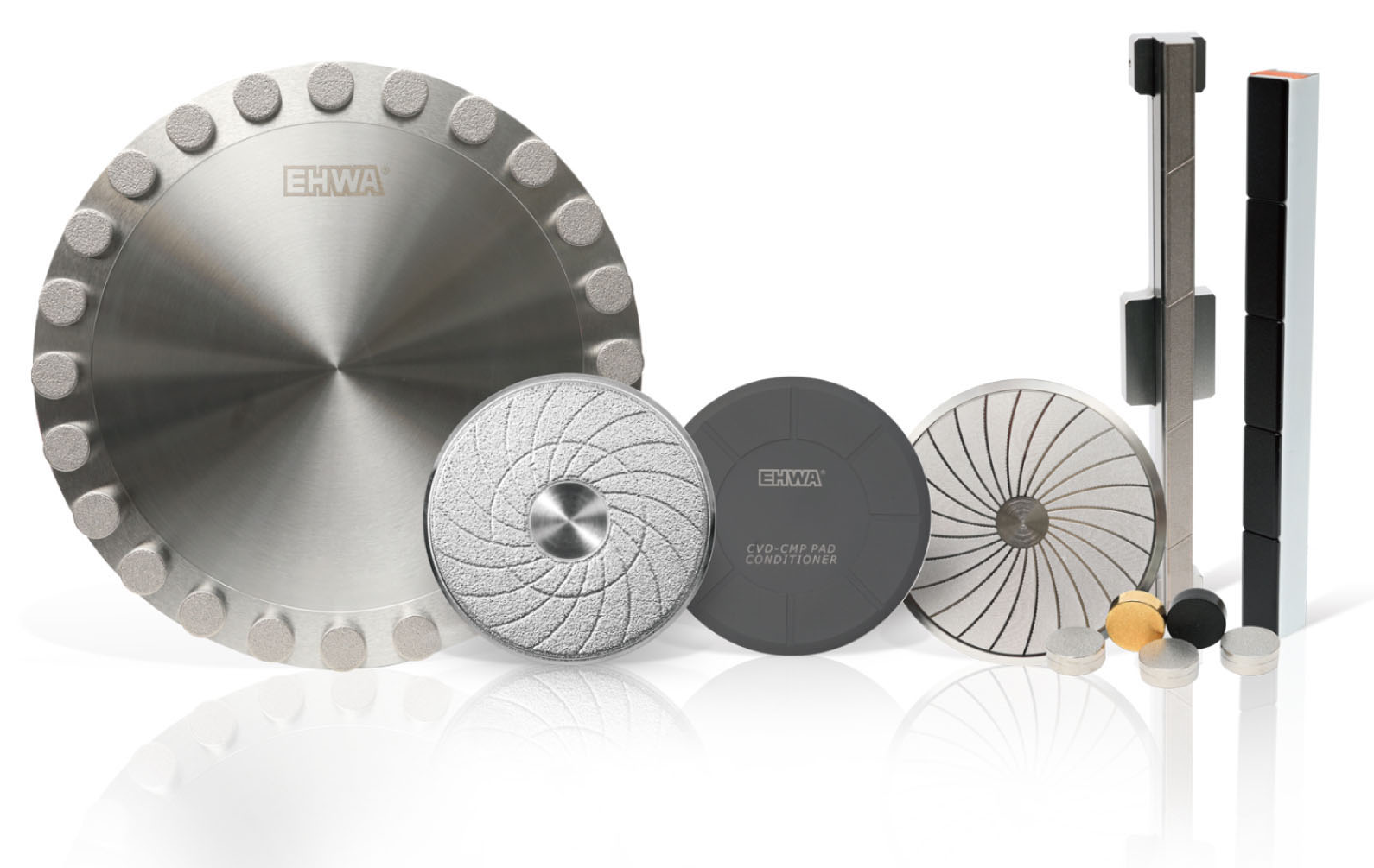
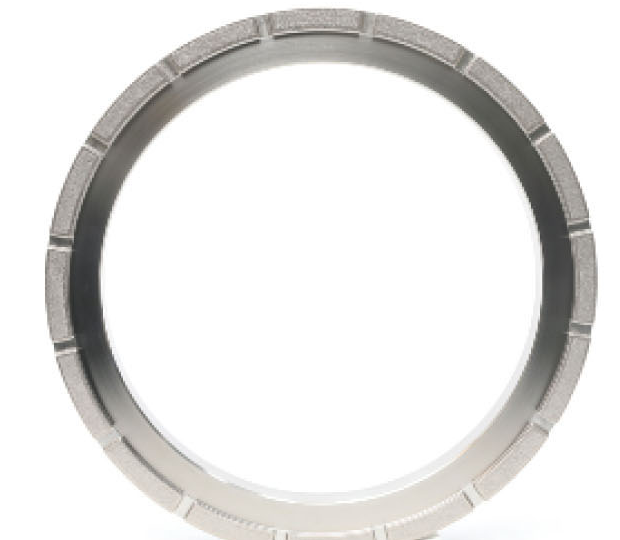
EHWA describes adapting BSL and CVD technologies to large conditioning tools, bar-type designs, rings and tools for existing CMP equipment. Product images show segmented bars, ring tools, discs with circumferential pellets and individual pellet variants. Front and oblique views illustrate tool form and segment arrangement.
BSL designs use chemical-mechanical retention and controlled diamond orientation for effective conditioning and free removal of pad debris. CVD provides consistently engineered tips and customisation of PCR, pad roughness and wafer removal. The particular working-surface concept is matched to available space, pad and process chemistry.
The large-format publications supplement the product views with the BSL-interface comparison and the protrusion/PCR comparison. These technical examples are presented in full in the preceding chapters. The tool forms extend the same working principles to different equipment configurations.
A tool designed for the required process can combine long use, consistent pad activation and economical consumption. Selection considers pad and slurry, polished material, equipment model, working-surface dimensions, mounting and the required PCR/roughness targets.
| Tool form | Illustrated designs |
|---|---|
| Bar | Upright view and pairs of segmented bars |
| Ring | Front and oblique views of segmented ring tools |
| Pellet disc | Large disc with circumferential pellets |
| Individual pellets | Different illustrated pellet variants |

Sources and application engineering
The trials and product ranges shown refer to the identified publication. Conditioner, pad, slurry and equipment settings are matched to the intended wafer process.
- EHWA: CMP pad conditioners, pages 1–17 (Q287).
- EHWA: CMP pad conditioners, pages 1–7 (Q217).
- EHWA: CMP pad conditioners, pages 1–7 (Q218).
- EHWA: CMP pad conditioners, pages 1–7 (Q229).
- EHWA: CMP pad conditioners, pages 1–7 (Q230).
- EHWA: CMP pad conditioners, pages 1–7 (Q234).
- EHWA: CVD CMP pad conditioners, pages 1–2 (Q002).
- EHWA: CVD CMP pad conditioners, pages 1–2 (Q017).
- EHWA: CMP pad conditioners, pages 1–2 (Q102).
- EHWA: CMP pad conditioners, pages 1–2 (Q103).
- EHWA: CMP pad conditioners, pages 1–2 (Q117).
- EHWA: CMP pad conditioners, page 1 (Q011).
- EHWA: CMP pad conditioners, page 1 (Q016).
- EHWA: CMP pad conditioners, page 1 (Q115).
- EHWA: CMP pad conditioners, page 1 (Q271).
Contact EHWA Europe for application engineering at info@ehwadia.de or +49 6173 997780.